UPTON, NY, Oct. 9, 2008 – The US Department of Energy’s (DoE) Brookhaven National Laboratory has reported that they successfully produced two-layer, superconducting thin films.
These nanoscale thin films exhibit superconductivity at their interface, rather than on their own. The research team has demonstrated the ability to elevate the temperature of superconductivity at this interface to temperatures exceeding -370 °F (50 kelvin), a relatively high temperature deemed more practical for real-world devices.
Such nanoscale superconductors would be useful in devices such as superconductive transistors and eventually in ultrafast, power-saving electronics.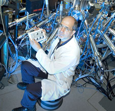
Ivan Bozovic, head of the Brookhaven thin film research team. Photo courtesy of the DoE's Brookhaven National Laboratory.
"This work provides definitive proof of our ability to produce robust superconductivity at the interface of two layers confined within an extremely thin, 1-2-nanometer-thick layer near the physical boundary between the two materials," said physicist Ivan Bozovic, who leads the Brookhaven thin film research team. "It opens vistas for further progress, including using these techniques to significantly enhance superconducting properties in other known or new superconductors."
Bozovic foresees future research investigating different combinations of non-superconducting materials.
"Further study of the temperature-enhancement mechanism might even tell us something about the big puzzle — the mechanism underlying high-temperature superconductivity, which remains one of the most important open problems in condensed matter physics," he said.
Bozovic's team had reported in 2002 the bizarre observation that the critical temperature (the temperature below which the sample superconducts) could be enhanced by as much as 25 percent in bilayers of two dissimilar copper-based materials. However, at that time, the scientists had no understanding of what caused this enhancement and in which part of the sample the superconductivity was located.
To investigate this further, they synthesized more than 200 single-phase, bilayer and trilayer films with insulating, metallic and superconducting blocks in all possible combinations and of varying layer thickness. The films were grown in a unique atomic-layer-by-layer molecular beam epitaxy system designed and built by Bozovic and his team to enable the synthesis of atomically smooth films as well as multilayers with perfect interfaces.
"The greatest technical challenge was to prove convincingly that the superconducting effect does not come from simple mixing of the two materials and formation of a third, chemically and physically distinct layer between the two constituent layers," Bozovic said.
Collaborators at Cornell University ruled out this possibility using atomic-resolution transmission electron microscopy to identify the samples' constituent chemical elements, proving that the layers indeed remained distinct.
"It is too early to tell what applications this research might yield, but already at this stage we can speculate that this brings us one big step closer to fabrication of useful three-terminal superconducting devices, such as a superconductive field-effect transistor," Bozovic said.
In such a device, one would be able to switch the transistor from the superconducting to the resistive state by means of an external electric field, controlled by applying a voltage and using the third (gate) electrode. Circuits built from such devices would be much faster and use less power than the current ones based on semiconductors.
"No matter what the applications, this work is a nice demonstration of our ability to engineer and control materials at sub-nanometer scale, with designed and enhanced functionality," added Bozovic.
For more information, visit: www.bnl.gov