Advances in CMOS sensors are providing a new choice for biological imaging.
Hank Hogan, Contributing Editor
When a rat decides on a course of action, you can’t ask it what factors played a role in that decision. But Jason Ritt, a postdoctoral fellow at the McGovern Institute for Brain Research at MIT in Cambridge, Mass., had to get as close as possible to doing that as part of basic neuroscience research.
Working with trained rats that responded one way to a smooth surface and another to a rough one, Ritt needed to know what in the movement of the rat’s whiskers provided the required information to the animal. That involved tracking whiskers moving about the same distance as their width a hundred times a second. What is more, those vibrations came in addition to the animal’s head movement, leading to certain imaging requirements. “You need to do not just good imaging but high-speed imaging,” Ritt said. He accomplished this goal with a CMOS camera from Cooke Corp. of Romulus, Mich.
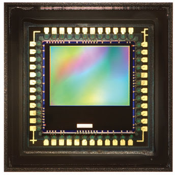
CMOS image sensors, such as this 3-megapixel offering from Micron Technology, are increasingly being found in life sciences applications. Advances have lowered the noise in such chips without compromising their wide dynamic range or image capture speed, two aspects of the technology that make it suitable for these applications. Courtesy of Micron Technology.
Ritt’s research is just one example of the application of CMOS sensors to biomedical and life sciences research. The list could be expanding thanks to sensor performance advances made in response to consumer demands.
Those advances are now being combined with innovative pixel design and low-noise readout circuitry. As a result, biomedical and life sciences research applications have a new tool in their arsenal, one that potentially can deliver the sensitivity of a CCD device but at far faster frame rates and perhaps for less cost. A look at various manufacturers shows how this CMOS wizardry is being done, while a canvas of end users shows how the new technology is being applied.
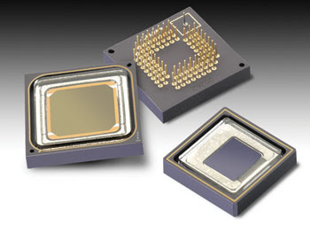
While some cameras for life sciences applications are based on standard CMOS sensors, others use chips customized in various ways. For example, Intevac Corp. thins down sensor chips significantly while they are still part of a silicon wafer. When in the camera, the chips are illuminated from the back side. This boosts low-light sensitivity substantially, according to company officials. Courtesy of Intevac Corp.
Ritt took the first step in his research with a CCD camera borrowed from another lab. With it, he subjected plucked whiskers -- measuring a tenth of a millimeter at their widest -- to tests that determined their mechanical characteristics while tracking the resulting movement. Although that camera worked for the evaluation phase, it would not for the next step. Next, he needed to image whisker vibrations as part of a freely moving animal, where the head of the rat might swing in any direction at a rate of centimeters per second. During that movement, whisker vibrations of a tenth of a millimeter with a frequency of hundreds of hertz had to be captured.
High resolution
“We needed a wide field of view at a high frame rate to measure very thin things. These are competing demands,” Ritt said.
The solution involved balancing the various needs, with the result that typically the data was captured at 3000 to 4000 fps. Also, it was a low-light situation, largely because the shutter speed is so fast. Ritt said that the first results are under review, with publication expected soon.
Emilia Entcheva, an associate professor of biomedical engineering, physiology and biophysics, and cardiology at Stony Brook University in New York, likewise needed speed along with a high pixel count. She and her coworkers were optically mapping electrical activity in engineered heart tissue to better understand the factors leading to cardiac arrhythmias.
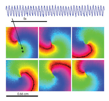
A spiral wave, a known precursor of lethal arrhythmias, in live cardiac cells is captured with an image-intensified CMOS imaging system based on a Cooke Corp. pco.1200 hs camera. Researchers used a calcium-sensitive dye and imaged the results at full resolution and at 200 fps. Courtesy of Emilia Entcheva, Stony Brook University.
“We use fluorescent dyes for voltage and calcium and employ high-speed high-resolution imaging,” she explained.
For this application, the need for high temporal and spatial resolution could be met only by an image-intensified CMOS-based solution. The resulting device has a data transfer rate of 1310 MB/s, temporal resolution of 500 fps and spatial resolution of 12 μm per pixel. That performance was not as good in terms of data throughput and spatial resolution as the researchers’ ideal detector, but it was better than any other solution presently available.
Both Ritt and Entcheva used the Cooke pco.1200 hs, which is based on a CMOS sensor from Micron Technology of Boise, Idaho, according to Cooke president Steve Daicos. It has 1280 × 1024 pixels and is the only CMOS-based camera made by the company. Its primary target is applications that need high resolution and high frame rates -- the camera provides up to 636 full frames per second. Even higher speeds are possible if only regions of interest are imaged.
The limiting factor in the speed is getting the data out of the device. So Cooke puts memory in the camera, with up to 4 GB of onboard memory allowing two to four seconds of full-speed, full-frame-rate recording. That data does eventually have to be read out, however. The device has a Camera Link option to provide faster transfers.
The company’s CMOS sensor also allows interframing -- the capture of two full frames with an interval as short as 70 ns between the snapshots. As a result, Daicos said, it can perform better microparticle image velocimetry, which is used to look at movement and flow within arteries and veins. The distance a particle moves from one frame to the next and the time between the frames yield the velocity and direction of the flow. A shorter interframe time means that higher-velocity particles can be tracked, extending the range of velocities over which the technique can be used.
New cameras with up to 16 GB are due to launch by the middle of the year. The new model will have 4-megapixel resolution and a 12-bit dynamic range, up from the current megapixel and 10 bits.
Daicos noted that current off-the-shelf CMOS sensors have about 85 electrons read noise, a rough halving of the sensor noise floor over the past five to six years. However, he said that CCD sensors still have better sensitivity than their CMOS cousins, although the gap is shrinking.
A new CMOS-based device is the ProgRes CT3 microscope camera from Jenoptik Laser, Optik, Systeme GmbH of Jena, Germany. The camera’s sensor has 2048 × 1536 pixels spaced 3.2 μm apart. It offers a 35-fps capture rate for a 682 × 512-pixel image. According to Jenoptik’s European sales manager Simon Schwinger, the sensor comes from Micron. “It is not the cheapest but offers the best performance for microscopy applications. And that’s what counted for us.”
The instrument has been out only since May, but Universidad Autonoma de Madrid biology professor Antonio Quesada already has plans to use it. Quesada heads a multidisciplinary group working on aquatic ecology. The group purchased the camera and a microscope to do bright-field, phase-contrast and fluorescence recording, but the work will not be confined to the lab.
“We will take the equipment to Antarctica to make the first screening of the biological diversity of microorganisms from remote places as well as identifying certain biological activities using also fluorescence,” Quesada said.
He noted that most of the group’s previous work has been done with a CCD-based system. The decision to try the new camera was driven largely by its specifications and reported performance. He and the other group members have limited experience with the new technology. They plan a series of trials comparing the new technology to the old. After assuring themselves of the performance, they will take the microscope and camera to Antarctica for field work from November 2008 to March 2009.
Thin is in
Of course, it is also possible to use a customized CMOS sensor, one that has been modified to improve performance. Santa Clara, Calif.-based Intevac Imaging does this by thinning a standard CMOS sensor via back lapping and selective chemical etching. The process substantially thins the standard CMOS wafer, which is ~600 μm thick.
According to Intevac’s director of business development, Leslie Tack, the result of this procedure enhances the device’s low-light sensitivity. “It can make the CMOS sensor anywhere from three to 10 times more sensitive,” he said.
This works, he explained, because the back side of the wafer is potentially more photoactive. The layer that captures photons and converts them into an electrical signal is buried in the silicon and beneath the circuitry. Thinning the wafer allows photons to reach this layer from the back. A bonus is that the fill factor -- the percentage of the pixel area that actively collects photons -- can be higher because there are no layers to block the incoming light. With back-side illumination, the fill factor can be 100 percent, as opposed to as low as 40 percent for front-side-illuminated sensors.
For the most part, the company sees its sensors as products for OEMs. However, it does make two cameras, the MicroVista-NIR CMOS near-infrared and the MicroVista-UV ultraviolet models. They have 1280 × 1024, 10.8-μm-pitch pixels and offer 30 fps imaging rates.
The near-IR camera is being used by Yingzi (Eliza) Du, an assistant professor at Indiana University-Purdue University Indianapolis, for biometric studies. One of the goals of the work is to perform iris identification on a subject who may be trying to hide his or her identity.
For such work, unobtrusive observation is important. That, in turn, leads to the need for particular sensor characteristics, which is why this equipment was chosen. “The product can provide better frequency response in near-IR frequencies, which is important for my research,” Du explained.
Another custom CMOS sensor is at the heart of the just-released NeuroCMOS-SM series cameras from RedShirtImaging of Decatur, Ga. The cameras have very large pixels, measuring 128 μm on a side and so having a 128-μm pitch. As a result, the fill factor is 70 percent, and each pixel has very deep wells. The cameras come in two array sizes -- 24 × 24 and 128 × 128 pixels -- and two maximum readout speeds -- 2500 and 10,000 fps.
The cameras are targeted at neuroscientists and cardiac physiologists, researchers who work with bulk-stained neurological and cardiac tissue. The fluorescence intensity of such tissue can be very high, and the deep wells and 21-bit dynamic range allow the camera to measure this intensity without saturating.
Lawrence Cohen is one of the founders of the company and a professor of physiology at Yale University in New Haven, Conn. In his own research, he studies the response to odors, looking at how the mouse and rat olfactory bulbs react to smells. He noted that the ability to spot changes in signals is important. “The signals in biological measurements are often very small fractional changes, down to 1 part in 10,000, so you need a large dynamic range.”
Cohen has tested the camera but not yet put it to use in his own lab. He added that CMOS sensors have made great strides in reducing read noise, with this sensor having a read noise of about 150 electrons. However, that’s still an order of magnitude higher than what is possible with a CCD sensor.
Embracing CMOS
High-performance imaging supplier Fairchild Imaging of Milpitas, Calif., manufactures everything from sensors to complete turnkey camera systems. As part of its portfolio, the company manufactures custom CMOS imagers. In doing so, it works with silicon foundries, customizing devices with low-noise readout circuitry.
According to Colin Earle, vice president of sales and marketing, this customization also involves engineering pixels so that they are the right size to optimize sensitivity and resolution for a particular application. If the pixels are too small, light-collection effectiveness is low, and the sensor won’t work well in a low-light situation. If the pixels are too large, resolution can suffer. In the case of typical optical microscopy, Earle said that the optimum pixel pitch is on the order of 6 to 7 μm. That is in contrast to consumer applications, where pixels run half that or smaller.
The recent improvements in CMOS imagers that make them suitable for scientific applications have been driven largely by the consumer market, according to Earle. Because the pixels on consumer CMOS sensors are becoming ever smaller, manufacturers of sensors used in cell phones and digital cameras are confronted by the continuous need to cut noise within the sensor. They have done so with process changes and through the implementation of architectures such as pin photodiodes.
Some significant strides have resulted, Earle said. “We’re seeing noise performance out of CMOS that is as good as or better than the CCD. Certainly we’re seeing speed capabilities out of the CMOS that are superior.”
The company came to this conclusion after developing a hybrid CCD-CMOS sensor. The goal was to match the imaging performance of CCDs with the readout speed of CMOS. While investigating the hybrid, Fairchild researchers kept tabs on CMOS performance and found that it had improved to the point where the need for the hybrid had largely disappeared. As a result, Fairchild Imaging is now concentrating on CMOS sensors for its next generation of products. The company has shuttered its CCD fabrication line and has become fabless.
This transformation of focus has happened because of a change in the technological landscape. Five years ago, if he had been asked whether CMOS sensors would largely replace CCDs in consumer, scientific and medical applications, Earle would have said that it might happen someday. “Today, I would say absolutely, and soon.”
How CMOS Imagers Work
Like CCDs, CMOS-based image sensors are semiconductor devices. Incoming light strikes a photosensitive area, where the photons free an electron. To do that, the photons must be energetic enough. In the case of silicon, that means they must be shorter than 1000 or 1100 nm in wavelength.
What happens after the electrons are produced distinguishes the two sensor technologies. In typical CMOS implementation, active amplification circuitry is connected to each photodetector, allowing active conversion of the accumulated charge into a corresponding voltage and digital signal within the pixel, which CCDs cannot do. In addition, a CMOS chip can read out pixels within an array by column- and row-selecting circuitry, which cannot be done with CCDs. The differences in amplification and readout account allow CMOS-based sensors to image faster and to consume less power.
However, the advantages of CMOS come at a price. The presence of circuitry reduces the photoactive area within a pixel. There also are nonuniformities in the amplifiers that could lead to uneven pixel response. When these factors are considered, CCDs offer better performance.
As for the relative noise occurring with each technology, Dalsa’s Cochrane said that, for short integration times (high frame rates), CMOS does well. For large pixels, CCDs beat the CMOS in noise, but for smaller pixels (around 5 μm and smaller), the CMOS is able to catch up, he said.
CMOS in Radiology
CMOS sensors are finding a home in another biomedical application as part of x-ray detectors. They can do so because the x-rays hit a scintillator that yields visible photons in response, and the sensors pick up that light. John Gilmore, a market research manager for Hamamatsu Corp. of Bridgewater, N.J., noted that the dental x-ray market has three segments: intraoral imaging performed on a routine basis to discover cavities; panoramic imaging, which images the entire mouth and jaw; and cone beam computed tomography (dental CT), which is three-dimensional imaging of the jaw, skull and, possibly, the ear, nose and throat regions. Most dental CT imaging is performed for surgical implants, but it is sometimes used for reconstructive surgery.
Hamamatsu supplies products to all three areas, with CMOS-based sensors primarily used in dental CT. One of the reasons for this is that the sensor is a monolithic device -- current versions measure 12 cm on one side -- and there are plans to develop a 12 × 24-cm arrangement.
The ability to obtain an acceptable yield from CMOS sensors at such large sizes is one reason why the company went with the technology. Another advantage is the sensor’s higher readout rate, a plus in dental CT because many images have to be taken.
Dalsa Corp. of Waterloo, Ontario, Canada, makes products for digital mammography and related x-ray areas. The company chose a CMOS sensor for these systems in part because the applications tend to produce abundant light. “Basically, medical x-ray is where we see a nice fit with CMOS,” said David Cochrane, Dalsa’s director of product marketing and management.