Exciting new findings about crystals –
on subjects as diverse as diamonds, peptide nanofibers and colloids – could
prove useful in science and industry, perhaps leading to new nanoscale constructs
and better electronics.
Diamond in extremis
Diamond has long been used to put the squeeze on other materials.
Now researchers have used lasers to return the favor, finding that a girl’s
best friend can support almost a million atmospheres. These results might lead to
better high-pressure science.
Previous static experiments indicated that, when the pressure
exceeds its strength, diamond deforms plastically, like a metal. The new results,
reported in the Jan. 22, 2010, issue of Physical Review B, show that, under dynamic
conditions, diamond acts like a brittle material.
There must be a transition between the two responses, and understanding
that could be key, said Lawrence Livermore National Laboratory physicist Jon H.
Eggert. “How this works is very important to the design of experiments using
diamond as a pressure generator.”
In their study, the researchers, from the University of California,
Berkeley, the University of Rochester in New York and the national lab, fired laser
pulses at diamond targets, using 100 GW of laser power at the Livermore Janus facility
and 3 TW on the Omega system at Rochester. The two produced nanosecond pulses of
532 and 355 nm, respectively.

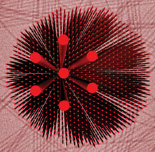
Laser pulses put pressure on a diamond sample. The bright white light is plasma, formed as a result of ablating
material with a laser to put force on the diamond. Courtesy of Eugene Kowaluk, Laboratory for Laser Energetics, University of Rochester.
They focused these down, ablated material they had deposited
on the surface for that purpose, and thereby created a shock wave in the diamond
sample. They used a high-precision imaging interferometer to measure Doppler-shifted
light reflected from the moving surface.
Future plans call for experiments to be done at the National Ignition
Facility at Livermore. There, the researchers can take advantage of the system’s
greater power and steadier laser-driven shocks to refine their understanding of
diamond.
Repulsive crystallization
Thanks to a serendipitous discovery, there is a new way to build
crystals. Investigators at Northwestern University in Evanston, Ill., showed that
it could be done using repulsion, instead of attraction. The finding could have
wide applicability, said research leader Samuel I. Stupp.
Repulsion brought about by x-ray exposure can cause crystallization under the right conditions. Foreground
illustration shows a highlighted hexagonal crystal lattice, formed when a peptide amphiphile (10-nm nanofibers in background) in aqueous solutions is subjected to x-rays. Courtesy of Honggang Cui and Samuel I. Stupp, Northwestern University.
“The mechanism of crystallization as a result of repulsive
electrostatic forces in confined systems such as on surfaces, in networks, in micron-scale
containers and so on could be used universally in synthetic materials as a way to
build structures.”
A professor of chemistry, medicine, and materials science and
engineering at the university, Stupp said that the new process was revealed when
the researchers applied synchrotron x-ray radiation to a solution of peptide nanofibers
they were studying. The solution underwent a dramatic change from clear to opaque,
and the x-ray signal showed crystallization occurring, something totally unexpected.
The same thing happened spontaneously at higher peptide concentrations,
the team reported in the Jan. 29, 2010, issue of Science, with separations between
filaments after crystallization of up to 32 nm. This self-assembly occurs because
of repulsive forces between nanofibers and their mechanical confinement in a network.
Something similar may be behind the construction mechanism of cytoskeleton filaments.
Applications of the new crystallization method could come in biomedical
therapies or in lithography. For example, it may be possible to build organized
nanostructures using x-rays, Stupp said.
Watching crystals grow – in a way
Building perfect crystals and thin films is important both for
commerce and research. Unfortunately, perfection is hard to achieve, and uncovering
what went wrong can be difficult because revealing the source of an error may require
watching atoms move on a surface.
To get around this problem, a group of researchers from Cornell
University in Ithaca, N.Y., scaled things up to make what was happening more visible.
In the process, they showed that random motions could play a critical role in constructing
crystals and thin films, something not clear before.
The researchers used colloidal particles in solution to model
atoms. Their study, which was reported in the Jan. 22, 2010, issue of Science, examined
epitaxial growth.
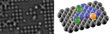
By watching a colloidal crystal form (A), researchers revealed the importance of diffusion, a result of the various barriers to particle movement around a step edge or a corner (B). Courtesy of Itai Cohen, Cornell University.
In their work, they made use of holographic optical tweezers,
said Itai Cohen, an assistant professor of physics. “We could take particles
to specific locations and then let them go. Using that technology, we could essentially
set up experiments at the single particle scale.”
Employing confocal microscopy, the researchers followed events
and showed that colloidal epitaxy obeys the same two-dimensional island nucleation
and growth laws that govern atomic epitaxy. They also determined the key role played
by particle diffusion in colloidal epitaxy. This previously ignored effect also
could extend to atomic systems because atoms get jostled by lattice vibrations.
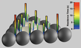
A residence time image for particles that were placed on top of a triangular island shows a measure of how long the particles would stay at a particular spot. Courtesy of Itai Cohen, Cornell University.
In the future, Cohen hopes that technological improvements
will allow researchers to follow the assembly of nanoscale particles. For now,
he noted that being able to tune the interaction between colloidal particles can
provide other important insights into physical systems.