
High-Precision Wafer-Level Optics Fabrication and Integration
Michael Kast, EV Group
The evolution of micro-optical components
for camera modules is today being strongly driven by the mobile phone industry,
while manufacturers of conventional camera modules – which are assembled from
a multitude of individual parts – are suffering from continuously decreasing
profit margins. Wafer-level fabrication and integration of micro-optical components
is a promising alternative that opens up a highly competitive route for camera module
manufacturing by using well-established microstructure technologies. The basic idea
is to use imprinting techniques to fabricate individual microlenses at the wafer
level; these are then continuously stacked by UV bonding until the ultimate optical
element is fully assembled. Finally, these elements are bonded onto the image sensor
at the wafer level, or a known good die approach is used.
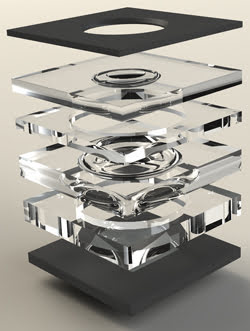
Elements of a typical wafer-level camera module include a CMOS image sensor, polymeric lenses
molded onto glass carriers by UV imprint lithography, spacers and aperture layers,
as shown in this exploded view. Images courtesy of EV Group.
Key advantages of wafer-level optics fabrication and integration
include the reduced form factor of the resulting wafer-level cameras and the highly
accurate assembly based on state-of-the-art imprint lithography and bond-alignment
technologies. Due to smaller form factors and lower cost-to-performance ratios,
wafer-level cameras have already begun replacing conventional barrel-type camera
modules. Key players, including Heptagon, Anteryon, Tessera, Aptina, Nemotek, Himax
and Visera, have successfully demonstrated the first wafer-level camera-based modules.
Market forecasts predict continually increasing demand, with wafer-level cameras
breaking 1 billion units per year within the next five to seven years. This trend
will be accompanied by the evolution of wafer-level cameras toward higher pixel
numbers, generating a need for more complex optical systems and, consequently, tighter
manufacturing tolerances.
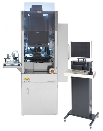
The EVG IQ Aligner is suitable for high-precision wafer-level optics
fabrication and integration of wafer sizes up of 300 mm.
Wafer-level optics fabrication
The starting point of each wafer-level optics manufacturing process
flow is master stamp fabrication. Wafer-level master stamps, which are based on
the design of the micro-optical component, must be fabricated for each individual
microlens contributing to the optical performance of the overall lens stack. The
most promising technique for master stamp fabrication is step-and-repeat ultraviolet
imprint lithography. The basic idea is to repeatedly replicate individual microlens
molds from a single lens master onto a master substrate, using a high-precision
alignment stage as a guide. Current step-and-repeat ultraviolet imprint lithography
technologies enable lens position accuracies of sub-100 nm, indispensable to meeting
future tolerance requirements of wafer-level camera modules. Besides producing high
uniformity of lens shape across the resulting wafer-level master stamp, step-and-repeat
ultraviolet imprint lithography accelerates materials evaluation and process optimization
for all relevant imprint processes due to its versatility in varying all relevant
process parameters during one individual process run.
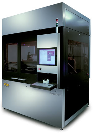
The EVG 770 NIL Stepper model for step-and-repeat
master stamp fabrication features positioning accuracies in the sub-100-nm range.
In the past 10 years, wafer-level UV molding of micro-optical
components has become the first high-volume manufacturing application of UV imprint
lithography since its introduction in 1995. This technique replicates microstructures
from a patterned stamp into an optical prepolymer using a combination of controlled
imprinting and UV-initiated polymer cross-linking. Polymeric working stamps are
commonly favored as stamp material, as they significantly reduce UV molding processes’
total cost of ownership. Moreover, release properties of working stamps can be tuned
to enable the defectless, repetitive demolding of lens wafers that is essential
for high-volume wafer-level optics manufacturing.
The most established wafer-level optics fabrication technique
is sequential double-sided microlens molding using puddle dispense. In this approach,
the optical prepolymer is dispensed as a single puddle onto the center of the wafer
via an integrated dispense system. Following overlay alignment of stamp and substrate,
the puddle is squeezed, which enables continuous filling of all lens cavities from
the center to the perimeter of the working stamp. Because of the nature of the imprint
process, a thin residual layer remains after UV imprint lithography, predetermined
by the final imprint gap. The key advantage of this approach is the ability to perform
all necessary process steps – including wedge error compensation, material
dispense, overlay alignment, controlled imprint, UV exposure and demolding –
on one dedicated equipment platform.
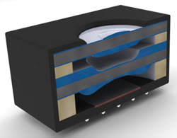
This cross section represents a fully assembled wafer-level camera
module. Polymeric lens elements (blue) molded onto glass carriers by UV imprint
lithography as well as spacer elements (yellow) constitute the micro-optics stack
sitting on top of the image sensor (red). The opaque housing (black) blocks unwanted
interfering stray light, which otherwise deteriorates the sensor response. The ball
grid array at the bottom of the module indicates the electrical contacts of the
image sensor.
An alternative UV molding technique is UV imprint lithography
using ink-jet dispense, in which the lens cavities on the working stamp are directly
filled with optical prepolymer by using ink-jet dispensers featuring pattern recognition
and autoalignment. During the subsequent imprint process, all individual lenses
are molded simultaneously as the stamp is touching the substrate at the interstitial
areas. This approach avoids creation of a residual layer, which significantly cuts
down on materials costs. And while ink-jet dispensers exhibit a much lower throughput
compared with puddle dispense, this is partly offset by the UV imprint lithography
systems’ shorter imprint times.
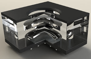
Shown is a cutaway of a fully assembled micro-optics stack bonded onto the image sensor.
Double-sided lens wafers and spacer wafers are repeatedly stacked by aligned UV
bonding until the total micro-optics stack is fully assembled.
In the final step, all individual lens wafers are stacked by aligned
UV bonding to form the ultimate micro-optics stack. The distance between adjacent
microlenses within the stack is adjusted using dedicated spacer wafers.
Image quality
The image quality of a wafer-level camera module strongly depends
on the manufacturing tolerances of the micro-optics stack sitting on top of the
CMOS image sensor. Key parameters include:
• Lens-to-substrate alignment
• Lens-to-lens alignment
• Lens stacking alignment
• Optics axis tilt
• Lens shape fidelity
• Thickness uniformity of bond interfaces
Each parameter must be addressed in the manufacturing process
to achieve the micro-optical system’s desired optical performance. In terms
of alignment, UV microlens molding and stacking processes have to be considered
as thick resist applications that necessitate dedicated proximity alignment procedures
realized in state-of-the-art UV imprint lithography equipment.
Also essential for high-precision wafer-level optics fabrication
are wedge error compensation routines, which literally compensate for any wedge
errors induced during UV molding or stacking processes by setting the wafer parallel
to the stamp. The imprint result strongly depends on the curing behavior of the
optical prepolymer. Significant shrinkage during UV exposure causes detachment of
the polymer from the stamp surface, which creates defects in the lens surfaces.
This effect can be eliminated by precisely controlling the imprint force that enables
microlens cavities to be constantly filled throughout polymer cross-linking. Finally,
the optical performance of the micro-optics stack depends on the uniformity of the
bond interface. This can be addressed by choosing a dispense technique that homogeneously
deposits the UV-curable adhesive.
At present, the camera module assembly generally uses well-established
semiconductor technologies to transition from discrete assembly to wafer-level integration.
Despite the significant reduction in camera module size made possible by wafer-level
optics technologies, the mobile phone industry demands thinner camera modules and,
thus, further miniaturization. In this context, the limiting factor inside a wafer-level
camera is the total sum of all constituting glass wafers, including individual lens
substrates and spacer wafers. A promising solution to overcome this limitation is
UV molding without a substrate. In this approach, the optical prepolymer is molded
between two stamps, similar to a Belgian-style waffle maker. Omitting the glass
carrier wafer adds more flexibility in the optical design, resulting in thinner
lens wafers and a total optical stack height that is significantly lower.
Wafer-level optics fabrication technologies are being considered
for other static optics applications, such as autostereoscopic 3-D displays and
high-brightness LEDs. Besides static features, dynamic ones such as adaptive optics
for autofocus are currently candidates for wafer-level manufacturing. The advantages
of this approach are similar to those for static wafer-level optics. Form factors
as well as manufacturing costs can be significantly reduced.
All above-mentioned technologies are considered to contribute
to the evolution of wafer-level optics as potential successors to conventional barrel-type
lens assemblies. As a consequence, equipment suppliers must be flexible, adapting
their dedicated equipment to the integration of highly customized processes related
to any of the above-mentioned concepts, and at a reasonable cost of ownership.
Meet the author
Michael Kast is product manager at EV Group’s headquarters
in St. Florian am Inn, Austria; e-mail: [email protected].
/Buyers_Guide/EV_Group_EVG/c4622