Compiled by EuroPhotonics staff
DUISBURG, Germany – Silicon nitride coatings block ultraviolet
and blue light, making image sensors ill-equipped for spectroscopy applications.
But a new production process renders the coatings transparent, making the sensors
suitable for special applications.
CMOS image sensors are no longer used only in cell phones and
digital cameras: They are making rapid inroads in high-performance applications.
For example, the automotive industry has discovered the potential of optical semiconductor
chips and is increasingly using them in driver-assistance systems – from parking
aids and lane detection to blind-spot warning devices.
In special applications, however, the sensors that convert light
into electrical signals must operate in difficult conditions such as high temperature,
moisture, mechanical influences and impurities. For this reason, CMOS devices are
covered with a silicon nitride coating applied in the final stage of production.
The coating process is called passivation and is now an industry requirement. Although
passivation addressed the temperature and moisture barriers, another problem needed
tackling: The silicon nitride coating limits the range of optical applications because
it is impermeable to light in the UV and blue spectral ranges.
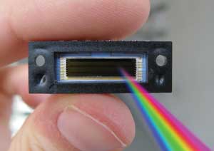
Scientists have developed a UV-transparent coating for image sensors. Courtesy of Fraunhofer IMS.
Scientists at Fraunhofer Institute for Microelectronic Circuits
and Systems have developed a coating that has the same properties but that is permeable
to blue and UV light. By increasing the proportion of nitrogen in the coating, they
reduced the absorption of shortwave light. They say the new coating material absorbs
less light of an energy higher than blue light, which means the sensors become more
sensitive at the blue and UV ranges.
To change the structure of the silicon nitride for the coating,
they had to fine-tune the deposition parameters such as pressure and temperature.
Their discovery has made CMOS image sensors suitable for use at wavelength ranges
down to 200 nm. Standard passivation allowed for a limit of only about 450 nm.
The range of applications for CMOS image technology now has expanded,
potentially revolutionizing UV spectroscopic methods that are used in laboratories
around the world. The sensors could play a new role in professional microscopy;
e.g., in fluorescence microscopes, they could provide scientists with images in
even greater detail.