Compiled by Photonics Spectra staff
The first true hybrid plasmon polariton nanoscale waveguides for next-generation on-chip optical communications systems have been demonstrated, which could hold great potential for nanophotonics, including intrachip optical communications, signal modulation, nanoscale lasers and biomedical sensing.
Scientists at Lawrence Berkeley National Laboratory (LBNL) have demonstrated the nanoscale waveguiding of light at both visible and near-infrared frequencies in a metal-insulator-semiconductor device that features low loss and broadband operation.
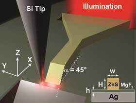
A hybrid plasmon polariton (HPP) nanoscale waveguide developed at LBNL consists of a semiconductor strip separated from a metallic surface by a low-dielectric gap. The schematic shows the waveguide responding when a metal slit at the input end is illuminated. Courtesy of Zhang group.
The group used a hybrid plasmon polariton (HPP) in a nanoscale waveguide system capable of shepherding light waves along a metal-dielectric nanostructure interface over sufficient distances for the routing of optical communications signals in photonic devices. The key to the system is the insertion of a thin low-dielectric layer between the metal and a semiconductor strip.
Until now, the size and performance of photonic devices were constrained by the interference that arises between closely spaced light waves; thus, the diffraction limit resulted in weak photonic-electronic interactions that could be avoided only through the use of devices much larger than today’s electronic circuits. A breakthrough came with the discovery that photons can be coupled with electrons by squeezing light waves through the interface between a metal/dielectric nanostructure whose dimensions are smaller than half the wavelengths of the incident photons in free space.

From left, Berkeley Lab’s Xiang Zhang, Ziliang Ye and Volker Sorger have demonstrated the first true nanoscale waveguides for next-generation on-chip optical communications systems. Courtesy of Roy Kaltschmidt, Berkeley Lab.
Directing waves of light across the surface of a metal nanostructure generates electronic surface waves (plasmons) that roll through the metal’s conduction electrons (those loosely attached to molecules and atoms). The resulting interaction between plasmons and photons creates a quasiparticle called a surface plasmon polariton (SPP), which can serve as a carrier of information. Hopes were high for SPPs in nanoscale photonic devices because their wavelengths could be scaled down below the diffraction limit, but problems arose because any light signal loses strength as it passes through the metal portion of a metal-dielectric interface.
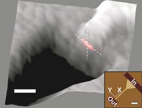
A three-dimensional overlap of the deep-subwavelength HPP mode signal (red spot) indicates the waveguide’s potential to create strong light-matter interaction for compact and highly functional photonic components. Courtesy of Zhang group.
To solve the problem of optical signal loss, the researchers proposed the HPP concept. A semiconductor (high-dielectric) strip is placed on a metal interface, just barely separated by a thin oxide (low-dielectric) layer. This new metal-oxide-semiconductor design results in a redistribution of an incoming light wave’s energy. Instead of being concentrated in the metal, where optical losses are high, some of the light wave’s energy is squeezed into the low-dielectric gap, where optical losses are substantially less compared with the plasmonic metal.
The scientists believe that prototypes based on this technology could be ready within the next two years and that the first products could be on the market within five years.
Their findings appeared in the May 31, 2011, issue of Nature Communications (doi: 10.1038/ncomms1315).