Compiled by Photonics Spectra staff
A new method that employs precise etching to produce miniaturized
thermal imaging sensors promises to enable large-scale manufacturing of automotive
safety devices.
Because they see more than the naked eye, infrared cameras could
improve traffic safety. They already are being used in the construction industry
and the military; however, infrared cameras are barely available in mobile applications
such as automotive safety systems because long-range infrared microsensors are difficult
to produce commercially in the quantities necessary.
Now, the Fraunhofer Institute for Microelectronic Circuits and
Systems (Fraunhofer IMS) has opened a facility to produce microsystem technology
(MST). MST involves minute sensors, valves or other mechanical components that are
integrated into semiconductor chips. In air bags, they serve as motion sensors.
To implement MST on semiconductors, the art of etching must be mastered, which is
where the scientists at Fraunhofer IMS come in.
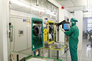
A researcher operates the production machine at Fraunhofer IMS’s new microsystem technologies laboratory and cleanroom facility. Courtesy of Fraunhofer IMS.
To apply the technology to a semiconductor, the scientists assembled
three layers. The lowest is a silicon wafer substrate, which is topped with a sacrificial
layer serving as a spacer and followed by a functional layer. The sacrificial layer
is later etched away, leaving only the desired sensor structure behind. The problem
is that traditional methods allow only vertical etching into the layers, said Marco
Russ, project manager at Fraunhofer IMS.
Unsupported structures are decisive for the mechanical functions
of many items of MST, he added, explaining that etching must work not only vertically
but also evenly in all directions, a process called isotropic etching.
This procedure ensures that the etching substance not only eats
vertically to the substrate, but also digs itself under the function layer. What
remains is an unsupported structure of the function layer that is only 100 nm thick
and connected to the substrate only at certain suspension points.
The conventional technique is to etch with liquids, which results
in the filigree membranes becoming glued to the substrate or even destroyed. Additionally,
most etching liquids do not permit the choice of just any combination of materials
for the function and sacrificial layers. The scientists said the new facility would
bypass these problems by using two different gases in the processing chambers of
the machine instead of fluids.
The gases are highly selective: Hydrogen fluoride has strong etching
properties on silicon dioxide but does not affect silicon. The exact reverse is
the case with xenon difluoride gas. The researchers can select which material is
better suited for the function layer.