Compiled by BioPhotonics staff
A semiconductor nanowire laser technology that can kill viruses,
purify drinking water and more has been discovered by scientists at the Bourns College
of Engineering at the University of California, Riverside.
Although widely used for biology, data processing and information
storage, ultraviolet semiconductor diode laser applications have been limited because
of size, cost and power. This breakthrough in zinc oxide nanowire waveguide lasers
offers smaller sizes, lower costs, higher powers and shorter wavelengths. Findings
appeared online July 3 in Nature Nanotechnology (doi: 10.1038/nnano.2011.97).
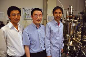
From left to right, scientists Guoping Wang, a graduate student,
Jianlin Liu, a professor of electrical engineering, and Sheng Chu, a graduate student,
developed a nanowire laser that can kill viruses or alter cells. Courtesy of University
of California, Riverside.
Until recently, zinc oxide nanowires could not be used in real-world
light-emission applications because of the lack of p-type material needed by all
semiconductors. Now, the researchers have doped the zinc oxide nanowires with antimony,
a metalloid element, to create the p-type material. Connecting the p-type zinc oxide
nanowires with n-type zinc oxide material, the scientists formed a p-n junction
diode. When powered by a battery, the nanowires emit highly directional laser light
from their ends.
The discovery could have a lot of impact. For biology and medical
therapeutics, living cells could be penetrated with the laser, or the nanowire laser
could excite or change a cell’s function from bad to good.
While the scientists have proved that p-type doping of zinc oxide
and electrically powered nanowire waveguide lasing works, they said that more work
must be done with the p-type material to make it more reliable and stable.