Plastics, glass, metamaterials, anisotropic materials – even smartphones – are teaming up to create a future where optical systems will be smaller, cheaper, lighter and more capable.
“Optical materials have gotten a lot better over the years,” said David J. Hagan, a professor of optics and physics at the University of Central Florida in Orlando. “They’re better understood.”
In particular, Hagan pointed to organics and plastics as areas where broader knowledge has brought improvement. One new material in this class that could be important in the future is a biologically inspired and inexpensive-to-manufacture polymer. The refractive index of optics built with the polymer can vary smoothly in three dimensions, and the resulting gradient index optics have applications in the military, in solar power and elsewhere.
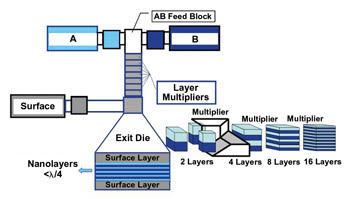
Fabricating biologically inspired gradient index optics involves co-extruding two polymers, A and B, in subwavelength nanolayers that make up 50-µm-thick films. These films form the basis for lightweight, inexpensive gradient index optics. Courtesy of Guy Beadie, US Naval Research Laboratory.
“One of the things we’re looking to do is to add this extra ray bending – this extra optical power – within the element to help improve imaging, to help reduce part counts, and reduce size and weight,” said Guy Beadie, head of the advanced optical materials section at the Washington-based US Naval Research Laboratory.
Studies have shown that putting gradient index polymers to work can reduce the volume and mass of lens designs by up to 50 and 90 percent, respectively. In part, the improvement is possible because the new materials are lightweight, but it also arises from their optical properties.

A mobile phone add-on consisting of low-cost optical materials enables quick and inexpensive eyesight testing. Such devices represent a new wave of optical material applications. Courtesy of MIT Media Lab, Camera Culture Group.
The Naval Research Lab and Case Western Reserve University in Cleveland are collaborating on work in this area. Scientists have developed a technique that extrudes thousands of layers of two polymers atop one another in a 50-µm-thick film. The repeated polymer pairs have a total thickness of 25 nm, well below the wavelength of light. Consequently, the resulting film is optically transparent with a refractive index between that of the two constituents. By altering the thickness of the base polymers within the fixed-unit cell during fabrication, researchers can create a library of intermediate refractive index films. These films can be stacked atop one another arbitrarily, molded, then polished into an optically clear lens with standard curved surfaces as well as an axial and radial gradient refractive index profile.
This capability can lead to some dramatic improvements, including allowing color correction to be done using one aspheric element instead of the two required by a homogeneous index material. A test comparing polymer to glass singlet lenses showed that the former decreased weight tenfold and offered better contrast.
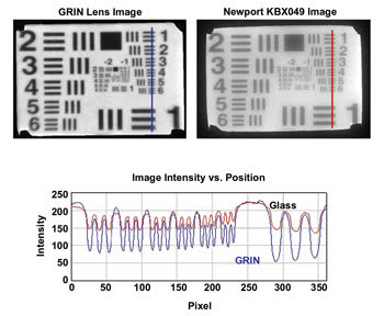
Polymer gradient index singlet lenses (above, left) weigh a tenth that of glass (right) but offer better contrast. Courtesy of Guy Beadie.
The polymer composite also enables new solutions. For example, Jeffrey M. Gordon, a professor at the Sede Boqer campus of Ben-Gurion University of the Negev in Israel, in collaboration with researchers at Columbia University in New York, outlined some results in January and August 2011 Optics Express papers. They showed that spherical lenses constructed out of gradient index plastics could concentrate incoming solar radiation more than a thousandfold onto a photovoltaic over the course of the day without having to track the sun.
However, it still would be necessary to move the photovoltaic about 2 cm to follow the shifting focal point, although everything else could remain still, Gordon said. This approach could be extended to wide-angle photography or infrared imaging.
Eric Baer, a Case Western Reserve professor, plans to extend the refractive index range from the current 1.5 to 1.6 out to 1.4 to 1.7. Work is under way to improve optical designs and associated software and to expand applications.
The Naval Research Lab’s Beadie predicted that polymer gradient index optics will have a substantial impact in the years to come. However, the new material will complement and not replace glass, he said. “The materials that we’re working with are plastic, and we’re not going to change the fact.”
Building better filters
As for glass, new knowledge has led to the development of a photo-thermorefractive variety. Through a combination of ultraviolet light and heat, it is possible to write a pattern of varying refractive index in such glass, said Leonid B. Glebov, a research professor at the University of Central Florida and vice president of research and development at OptiGrate, a startup formed to commercialize the new material. Both are in Orlando.
Lasers and heat allow refractive index patterns to be written throughout the bulk of photo-thermorefractive glass, leading to narrow-spectral-width filters and other optical components. Courtesy of Leonid B. Glebov, University of Central Florida and OptiGrate.
The glass is transparent from 220 to 2700 nm, and features that measure tens of nanometers in size can be written into it. A key point is that, although lasers initiate the process, the image actually is formed by heat. Thus, the resulting pattern cannot be bleached or altered by light, making it possible to subject it to high-power lasers without damage.
OptiGrate makes spectral filters using the glass. The ability to produce interference-derived filters throughout centimeters of glass offers an advantage because spectral selectively goes up with thickness. The company’s filters offer rejection coefficients of up to 10,000 to 1, and the spectral width of what is allowed through is only 20 to 30 pm, Glebov said.
“This is an order of magnitude narrower than any other commercial filters,” he noted.
That translates into better spectroscopy. Applying the same techniques to the output coupler for a laser allows spectral brightness to be increased hundreds of times, achieved by narrowing the output to a 30-pm spectral width without losing power. The glass allows beams to be locked to a wavelength, or several beams to be combined into one, he said.
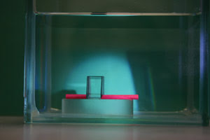
Invisibility through anisotropy: A rolled-up piece of paper sits under a cloak wedge made of calcite, a material with direction-dependent optical properties. The portion of the object inside the wedge is not visible, and the wedge surface appears to be flat, creating a cloaking effect. Courtesy of Baile Zhang and George Barbastathis, SMART Centre, Singapore.
A future research direction is to make narrower and narrower filters, he added. Another area of investigation involves the production of multiple holographic patterns in a single piece of glass.
Less-metallic metamaterials
Metamaterials, the stuff of invisibility cloaks and superlenses, represent a third novel optical material. The electromagnetic characteristics of the source materials and their physical arrangement allow optical properties to be engineered. As a consequence, the resulting refractive index can be below 1 or even negative, something unknown in nature.
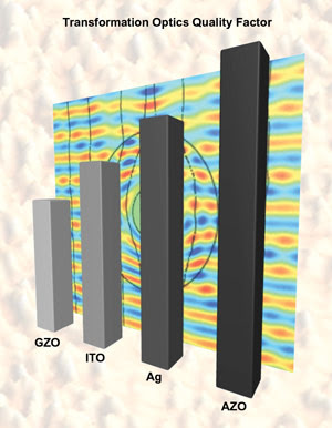
Not all that glitters is gold or silver, at least for visible and near-infrared metamaterials. The chart shows the quality factor of various metamaterial candidates, with a higher bar indicating better quality resulting from lower losses at the plasmonic crossover frequency. The materials are, from left to right, gallium zinc oxide (GZO), indium tin oxide (ITO), silver (Ag) and aluminum zinc oxide (AZO). Crossover frequencies are, respectively, 1.32, 1.69, 0.326 and 1.3 µm. Courtesy of Alexandra Boltasseva and Paul West, Purdue University.
There are signs that metamaterials are moving out of strictly academic labs. For instance, defense contractor Lockheed Martin Corp. has turned to metamaterials to boost the performance of spacecraft antennas. Last year, a research lab at Wright-Patterson Air Force Base in Ohio sought a contractor to help develop metamaterials for optical filters, time-domain optical components and other areas.
But all current metamaterials suffer from a basic problem, said Alexandra Boltasseva, an assistant professor of electrical and computer engineering at Purdue University in West Lafayette, Ind. Silver- and gold-based metamaterials suffer high losses at optical frequencies, so she is advocating – and is now investigating – a basic material change.
“We are trying to move to materials that can still provide us with these metallic properties but that will have lower losses,” she said. In electronics, when you need something that is metallike but not a metal, you turn to semiconductors. Similarly, Boltasseva is looking into wide-band semiconductors, such as doped zinc oxide or indium tin oxide.
Semiconductor fabrication techniques can create structures well below the wavelength of interest, a metamaterial requirement. There also is a large semiconductor manufacturing base, potentially allowing inexpensive production of any optical component.
Another approach is to use new materials, one possibility being intermetallics such as titanium hafnium nitride. Stacked layers of alternating materials such as these could lead to constructs with acceptable losses and negative refraction in the visible or at 1.5 µm, a wavelength important in telecommunications. Further down the road would be metamaterial devices with properties that could be adjusted by applying voltage, a possibility enabled by semiconductors.
As for applications, some would require optimizing devices, but an immediate use would be in microscope optics. A superlens offering better-than-diffraction-limit imaging was demonstrated by a group from the University of California, Berkeley, in 2005 using silver, a current metamaterial.1 But the metallic nature of the construct keeps it from being used in an objective because of high losses and fabrication challenges. That wouldn’t be the case for a superlens constructed with a transparent semiconductor. That alone makes the successful debut of a semiconductor metamaterial an important event to watch for over the next few years.
“As soon as we can demonstrate such a structure based on semiconductors, there would be immediate interest and immediate steps toward a real-life application,” Boltasseva said.
Invisibility by another path
There is, however, another avenue to invisibility. It exploits optical anisotropy and directional differences in optical properties, and it represents another class of novel optical materials. Researchers at MIT in Cambridge and the Singapore-MIT Alliance for Research and Technology Centre in Singapore showed that calcite, a common material, could render 2-mm-tall objects invisible under the right conditions. They described the setup in a January 2011 Physical Review Letters paper.
The focus now is not on invisibility but rather on a related concept – manipulating the trajectory of light – said team leader George Barbastathis, Singapore research professor of optics and MIT mechanical engineering professor. This may be for specific wavelengths, such as those involved in telecommunications.
“We’re interested in other applications where you have to shield certain devices from light,” Barbastathis said. “For example, in integrated optical circuits, very often one wants to prevent certain parts of the circuit from being illuminated.”
Although anisotropic materials occur naturally, they also can be engineered via nanopatterning, Barbastathis said. And because the material is otherwise homogeneous, it should be easier to fabricate than alternatives.
Finally, a class of novel optical materials is not material at all. An example is a lensless holography microscope demonstrated by researchers at the University of California, Los Angeles. The field-portable device offers lateral resolution of better than 2 µm over a field of view of about 24 sq mm. Aydogan Ozcan, an associate professor of bio- and electrical engineering, headed up the project, which was described in an August 2011 paper.
In one mode of operation, the device reflects a laser off a specimen, and this light interferes with a separate reference beam at a digital sensor array. This data is filtered to remove unwanted information, and a computer then digitally reconstructs an image of the specimen. The device also has a transmission mode.
The light weight and low cost of the device would be particularly beneficial during field work in the developing world. Possible applications include screening of blood for pathogens or testing of water quality. For such uses, what is needed sometimes is a microscope with adequate resolution but a very wide field of view because what is being searched for is not common.
“If you look at malaria slide readings, it’s a rare event problem. Around 1 percent of the red blood cells show malaria signatures,” Ozcan said.
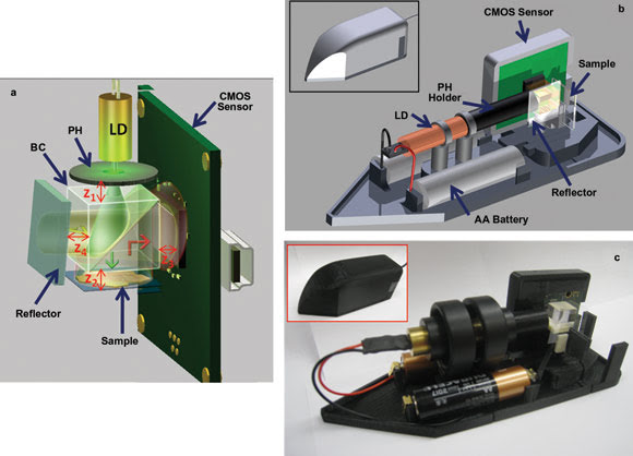
Using sensors, a laser diode (LD), holography and image processing, researchers built a compact, lens-free microscope suitable for field work. Concept is shown in (a), artist’s rendering in (b) and actual device in (c). Reprinted from Biomedical Optics Express. Courtesy of Aydogan Ozcan, University of California, Los Angeles.
He added that extensions to the idea involve lens-free fluorescence imaging and resolution improvements at the submicron level. Along with others, he has formed a company, Holomic LLC, to commercialize the concept.
Optical materials and the phone
Such efforts point the way toward an increasingly important factor that affects optical materials – and vice versa. The advent of smartphones promises to change microscopy, spectroscopy and other areas because smartphones have high-resolution displays, megapixel cameras, storage and connectivity, and they offer powerful local computing. When combined with simple attachments, they can make surprisingly capable microscopes and other optical devices.
An example can be seen in the work of Ramesh Raskar, an associate professor at the MIT Media Lab. While developing a new bar-code system, he realized that it could be used to make a refraction map of the eye, something traditionally done by a doctor when figuring out an eyeglass prescription.
This mapping now can be done using a smartphone and an inexpensive attachment. Software creates a carefully arranged pattern of lines or dots on the display, and then it puts the patient to work.
“We ask the user to create changes in the position of the dots,” Raskar said.
The adjustments reveal refractive distortions in the eye. Because uncorrected vision problems are a leading cause of blindness for millions worldwide, such a device could be very beneficial. That’s the idea behind EyeNETRA, a company formed to commercialize the concept. Vitor Fernando Pamplona, a graduate student who was at the MIT Media Lab and is now at Brazil’s Federal University of Rio Grande do Sul in Porto Alegre, developed the smartphone eye doctor technique as part of his thesis and is involved with EyeNETRA.
When it comes to getting the device into the field, Pamplona said one idea would be a microbusiness model, with people in large cities in the developing world paying for the ability to run a set of tests. These buyers would then travel to the countryside, where they would perform an eye exam in return for payment. The test itself would likely be an aide, helping people decide whether they need to see a doctor.
Other vision problems also could be discovered by a similar combination of a smartphone, an attachment, software and the right techniques. Pamplona demonstrated that this setup can be used to find cataracts, something done today with a machine developed nearly 50 years ago and that can take months to master. The fact that a phone can match its performance isn’t that surprising, given the technology available.
“The sensors we have on the phone right now are pretty good,” Pamplona said. “They’re reaching a scientific level, a professional level, in the sense it is comparable with high-end specific tools. So you can start building on top of them.”
Because the phones are being used in medical devices, there are regulatory issues to consider that might keep them from being deployed soon. Getting approval for a new medical device from the FDA, for example, is expensive and takes time. Thus, phone-enabled devices might first show up in areas where the lack of access to health care makes them more compelling.
An even wider array of optical materials and techniques in even more settings looms on the horizon. Pamplona foresees a day when 3-D printers make it possible to whip up a phone attachment on demand, allowing users to download needed software and hardware to perform optics-based tasks.
Another example of a smartphone-based approach comes from Sebastian Wachsmann-Hogiu. An associate professor and facility director of the National Science Foundation’s Sacramento-based Center for Biophotonics Science and Technology, part of the University of California, Davis, he has done microscopy and spectroscopy using phones for point-of-care applications. The work was described in a March 2011 PLoS One paper.
Wachsmann-Hogiu has identified various blood diseases using inexpensive optical components and a phone. He is working with industry partners to commercialize these techniques. Many more applications from researchers and companies could follow, affecting many areas. “Ten years down the road,” he said, “cell phones will likely play a significant role in medical diagnosis in general. Microscopy and spectroscopy are only two possible ways. There are other things that can be done.”
Reference
1. N. Fang et al (2005). Sub-diffraction-limited optical imaging with a silver superlens. Science, Vol. 308, pp. 534-537.