LED makers strengthen the appeal of their products by adopting a semiconductor-industry-type approach to yield management, defect control and dedicated manufacturing equipment.
Compared with semiconductor fabrication, LED production is still in its adolescence. Manufacturing yields remain extraordinarily low – in the region of 30 to 40 percent – according to a recent report by market analysis firm Yole Développement of Lyon, France.
But there is change afoot as LED manufacturers transition to a more mature, semiconductor-industry kind of philosophy. Instead of using old-generation repurposed semiconductor equipment (which delivered subpar yields and performance), LED makers are now installing dedicated equipment optimized for LED manufacture.
“We’re now seeing dedicated lithography, PECVD [plasma-enhanced chemical vapor deposition], dry etching and PVD [physical vapor deposition] tools delivering optimum cost of ownership,” said Dr. Eric Virey, Yole Développement’s senior market and technology analyst of LED materials and services. “We’re also seeing increasing adoption of semicon manufacturing best practice in terms of yield management, defect control, [statistical process control], etc. This should further improve yields and manufacturing efficiency while decreasing cost.”
All of the leading LED companies are upping their game, including Osram Opto Semiconductors, Cree, Philips Lumileds, Nichia, Toyoda Gosei, Samsung, LG, Epistar, Formosa Epitaxy Inc. and a few of the new emerging forces in China such as Sanan Optoelectronics Co. Ltd.
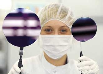
Osram Opto Semiconductors demonstrates 6-in. chip fabrication (left) and 4-in. chip fabrication (right). Courtesy of Osram Opto Semiconductors.
Bigger is better
Until recently, the majority of LEDs were fabricated on 2-in. sapphire wafers, and the past few years have seen some companies move to 3- or 4-in. wafers. This year, however, there has been a significant transition toward even larger diameters, with many companies in Taiwan adopting 4-in. wafers while some technology leaders like Philips Lumileds, Osram Opto Semiconductors, Toyoda Gosei and LG are manufacturing on 6-in. wafers, according to Yole’s report.
“Larger diameters typically allow sizable cost saving and equipment throughput but pose significant challenges in terms of technology and process – which explains why it took so long for many companies to make the jump,” Virey said. “Also, prices of the smaller-diameter wafer have dropped dramatically in the last 18 months.”
Germany’s Osram Opto Semiconductors was one of the first companies to transfer to 4-in. wafers for all material systems in 2006. Then, in 2011, it was among the first to start production on 6-in. wafers.
Another important trend in recent years is high-volume production, as Dr. Matthias Sabathil, director of advanced concepts and engineering at Osram, pointed out. “Standardized products and product platforms did make this possible. Both these manufacturing trends support the worldwide need for less-expensive LEDs – new materials, optimized processes, volume production and package platforms.”
Sapphire versus silicon
The use of patterned sapphire substrates (PSS) is now widespread, and it is thanks to micronscale patterned wafers that the brightness of LEDs has significantly increased. In fact, Yole’s report reveals that some companies are now looking at nano-PSS to further increase performance in terms of light extraction and also, possibly, internal quantum efficiency and electrical properties.
Although an estimated 80 percent or more of LEDs are now made on PSS, most of the leading LED makers, including Bridgelux, Toshiba and China’s Lattice Power, are looking to replace sapphire substrates with silicon.
Silicon substrates would open the door to manufacturing 8-in. wafers and potentially could reduce front-end cost (chips) by up to 60 percent by manufacturing on cheaper wafers and using existing, highly automated and fully depreciated CMOS facilities.
But silicon poses a new set of challenges, and silicon wafers are prone to bowing and layer cracking, both of which strongly affect yield. While engineers are busy devising stress management layers to mitigate these issues, it remains to be seen whether LED on silicon can be mass-manufactured with yields and performance that are high enough to deliver the promised cost savings.
Cost saving is the ultimate goal of companies such as Soraa in the US, Seoul Semiconductor in South Korea, and Panasonic in Japan, all of which are considering GaN wafers for LED fabrication. Although 100 times more expensive than sapphire wafers, GaN performs much better when driven with a high current.
“This means that the higher substrate cost can potentially be offset in some application[s] by reducing the number of LED[s] needed to produce [a] large amount of light over a small surface,” Virey said. “For example, spotlights, projection applications [and] headlamp automotive lighting.”
Phosphor research blooms
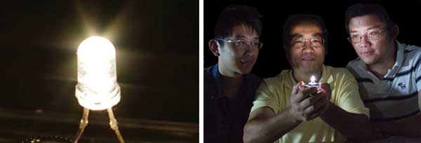
While emitting the ideal radiance for automotive lighting and for backlighting of liquid-crystal televisions, white LEDs are not as palatable indoors. Most of the commercialized white LEDs are made by combining a blue LED chip with a yellow phosphor, which, while highly efficient, produces a cool, bluish-white light and lacks a sufficient red spectral component.
In a bid to develop warm-white light with good color rendition, research into new phosphors has expanded. Associate professor Zhengwei Pan at the University of Georgia in the US, recently published a paper in Light: Science & Applications about his work developing a yellow phosphor with single-emitting center for warm-white LEDs.
Many new phosphors emitting blue, green, yellow and red (or orange-red) light have been synthesized. Most of the phosphors are based on luminescent ions of Eu2+ and Ce3+, whereby the emission color of the two ions is tunable depending on the host materials in which they are incorporated.
“Different types of host materials have been developed, including aluminates, silicates, sulfides and nitrides,” Pan said. “Currently, the most promising ones include Eu2+-activated green- and yellow-green-luminescent silicates; Eu2+-activated green-luminescent oxynitrides; and Eu2+-activated red- or orange-red-luminescent nitrides. All can be used to achieve warm-white LEDs through the multiphosphors-conversion model.”
Pan and his colleagues have developed a yellow barium europium aluminate (Ba0.93Eu0.07Al2O4) phosphor with a single Eu2+-emitting center that emits warm-white light with high color rendition when singly combined with a blue LED.
The use of a single phosphor with a single-emitting center is more reliable than, say, using a single phosphor with multiemitting centers or using multiple phosphors. This is mainly because different emitting centers generally exhibit different thermal quenching behaviors of luminescence, which decreases the color stability of the final white LEDs.
“Generally speaking, the single-phosphor, single-emitting-center-conversion model represents the ideal way for fabricating warm-white LEDs because it is reliable and free of emitting-color stability concerns,” Pan said. “For the multiphosphors-conversion model, while highly efficient blue, green and green-yellow phosphors are available, efficient orange-to-red phosphors are still [lacking]. So, new efficient orange-to-red phosphors are needed.”
Single-phosphor, single-emitting-center-converted white LEDs are being explored for their warm-white light quality and good color rendition for indoor illumination. Courtesy of the University of Georgia.
Pan’s team will now address the issues of low efficiency and low yield production suffered by the new phosphor. “These drawbacks must be addressed in order for Ba0.93Eu0.07Al2O4 to become a very competitive candidate for general illumination applications,” Pan said.
Osram Opto Semiconductors is continuously working to improve its existing inorganic phosphors and at the same time keep an eye on novel materials such as semiconductor converter quantum dots, organic phosphors or materials based on novel ceramics.
“Quantum dot phosphors offer a narrow spectrum and enable highly brilliant colors – and this is very interesting for backlighting applications,” Osram’s Sabathil said. “Ceramic phosphor materials are ideal for high temperatures and high flux. They offer good opportunities for high-performance applications like automotive headlamps or LED projection.”
Although initially plagued by low-lifetime and high-temperature performance, quantum dots have come a long way, and the first commercial applications are emerging.
The LED promise
Light manufacturers need to appreciate the growing importance of optics design and manufacturing as well as the need for very precise optical elements in LED production if they are to confirm the merits of LEDs, said Dr. Peter Schreiber of Fraunhofer’s Institute for Applied Optics and Precision Engineering (IOF) in Jena, Germany.
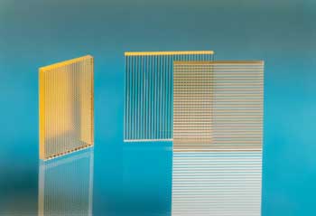
Beam divergence conserving diffusers (micro-optical fly’s eye condensers), replicated into polymer on glass. Courtesy of Fraunhofer IOF.
“With efficient optics, we have the opportunity to prove the promise of efficient lighting,” Schreiber said. “But, for the small LED chips, we need also small but precise and precisely mounted optics. This requires some changes of mind of the luminaires manufacturers – which are used to work[ing] with large, not-too-delicate optical components.”
In terms of general lighting, there is a need for free-form optics for directing the light into arbitrary irradiance distributions as well as a growing demand for diffusers.
Inhomogeneous light sources such as LED clusters, which are particularly critical for clusters of chips with different colors or color temperatures, will “form a homogeneous irradiance distribution without artifacts of the source geometry,” Schreiber said. “Currently available diffusers suffer from broadening of divergence, changing color with angle, and low transmission.”
To open the door to massive adoption in lighting applications, LED cost must be lowered while performance improvements are maintained. Virey predicts that a trigger point will be reached this year and that sizable adoption of LEDs will be seen in some geographic areas: “where the stars are aligned – i.e., with high energy cost, mandatory phaseout of low-energy-efficiency light source[s] like incandescents, and good consumer awareness of the benefits of LEDs.”