Nanophotonics is now a major research theme in optical physics and engineering. Driven by the dream of untapped device functionality, nanophotonics studies the exciting science of the interaction of light with nanostructures, at the size scale where optical, electronic, structural, thermal and mechanical properties are deeply interdependent.
Some experts believe that nanophotonics will continue to boom for the next decade on the ticket of a green enabling technology, and that with an outlook of 10 years plus, we will see “nanophotonics inside” solutions for telecoms, sensor and data-processing applications.
“We are now living in an exciting epoch of science and technology that witnesses an accelerated convergence of various research fields and technologies at multiple levels,” said Dr. Tuan Vo-Dinh, director of the Fitzpatrick Institute for Photonics and professor of biomedical engineering and chemistry at Duke University in Durham, N.C. “Nanophotonics is an element of this momentous convergence occurring at the intersection of photonics and nanotechnology.”
Materials fabricated on the nanoscale display some intriguing properties when it comes to interaction with light.
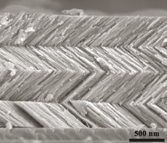
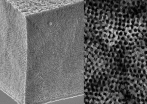
A scanning electron micrograph of a sculptured thin film (STF) with chevronic morphology, made by evaporation of a chalcogenide glass at Pennsylvania State University. STFs are useful as nanophotonic filters and as optical surface waveguides for long-range communication. Photo courtesy of Akhlesh Lakhtakia.
“Nanoscale materials possess a lot of surface area in relation to volume. Therefore, processes that occur on surfaces dominate processes that take place in volumes,” said Dr. Akhlesh Lakhtakia, professor of engineering science and mechanics at Pennsylvania State University. “Nanoscale materials affect light differently than bulk (dense) materials.”
Quantum optics and plasmonics
Molecular factory processes and nanofabrication have led to the development of species, materials and products at the nanometer scale. This new class of optical nanostructures includes photonic crystals or photonic bandgap materials that have been developed to transmit and store photons at subwavelength scales in free space.
At the lower end of the nanoscale, quantum effects begin to dominate – and the quantum dot emerges. Quantum dots have very pure colors and can be used for high-clarity displays, for imaging biological objects and for enabling drastic advances in quantum optics and quantum information communications and processing.
A single layer of nanoparticles of gold has a peculiar color. Stretching the layers increases the gap between the nanoparticles, changing their color, as electrons find it harder to hop between the nanochunks of metal. Photo courtesy of Matthew Millyard, NanoPhotonics Centre, Cambridge University, England.
Nanoparticles of plasmonic materials such as gold and silver – nanoplasmonics – enable enormous electromagnetic enhancements. This means that they can be used to concentrate electric fields, enabling ultrasensitive detection in medical diagnostics, and possibly leading to more efficient thin-film solar cells.
In combination with optical traps, plasmonics can enable scientists to investigate biological systems such as single proteins and cells. By studying their interactions with plasmonic nanostructures, hard-soft matter connections such as brain-computer or mind-matter interfaces can be better understood.
Duke’s Vo-Dinh has been investigating plasmonics-active nanomaterials and nanosensing technologies for more than three decades and, in 1984, was the first to report the general applicability of surface-enhanced Raman scattering (SERS) as an analytical technique relevant to a wide variety of chemicals, following the SERS observation by other groups.
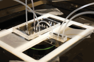
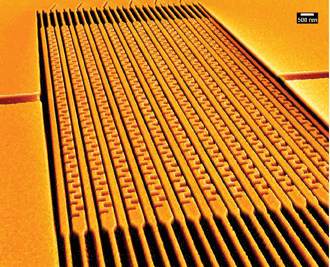
Sticking together gold nanoparticles chemically with precise subnanometer gaps offers a new way to trap light into volumes much smaller than their wavelength. The intense light field can then be used for sensing inside these microfluidic devices, which scoot tiny bubbles of water around the sensing chip. Photo courtesy of NanoPhotonics Centre, Cambridge.
Since then, his laboratory has developed nanobiosensors capable of probing physiological parameters (pH), detecting individual biochemical species (DNA adducts) and monitoring molecular pathways (apoptosis) in a single living cell.
“These nanosensors lead to a new generation of nanophotonic tools that can detect the earliest signs of disease at the single-cell level and have the potential to drastically improve our fundamental understanding of the life process of the cell,” Vo-Dinh said. “Unique metallic nanoprobes have been designed for early detection of various diseases (cancers, infectious diseases, etc.), for use in in vitro diagnostics and in vivo biosensing applications.”
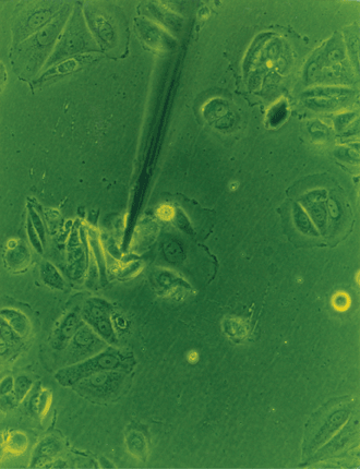
A fiber optic nanosensor with antibody bioreceptor monitors biotargets in a single cell. Photo courtesy of Dr. Tuan Vo-Dinh.
But it’s not just sensing applications that can benefit from plasmonics research. Disease treatment could also get a boost from a new plasmonic platform dubbed gold nanostars. Nanostars have small core sizes with multiple long, thin branches that exhibit intense two-photon luminescence and high absorption cross sections.
Because nanostars are tunable in the NIR region with a relatively low scattering effect, they are ideally suited as photothermal nanoagents in cancer therapy, Vo-Dinh said.
“We hope that the nanophotonic systems using plasmonic nanomaterials and biosensing technologies will contribute to bringing a bright future to biochemical and medical research and could ultimately lead to the development of new modalities of environmental sensing, bioimaging, high-throughput screening, early diagnostics, drug discovery and medical treatment,” he said.
Imaging and sensing on the nanoscale
Nanophotonics is an enabling technology for a myriad of far-reaching practical applications, including a variety of unique optical sensing and imaging techniques such as near-field spectroscopy, far-field superresolution microscopy and STED (stimulated emission depletion) fluorescence microscopy.
Such techniques have proved important for investigating materials and biological systems at the nanoscale, giving insight into the cell machinery and intimate life processes occurring at the molecular level that previously were invisible to human inquiry.
Thanks to nanosensors – which can detect single molecules – used with optical molecular probes, biochemical processes can be tracked within intracellular environments in vivo. The molecular nanoprobes allow detection of the earliest signs of disease at the genetic, molecular and cellular levels, leading to early detection and effective therapy.
And when it comes to treatment, nanocarriers (molecules that have their shells conjugated with antibodies) allow for targeted delivery of drugs, and plasmonics-active nanoprobes can be used for remotely triggered light therapy (photothermal therapy, photodynamic therapy).
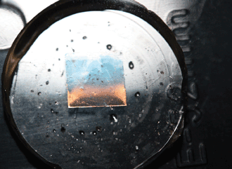
These 3-D interconnected meshes of gold give light pause to think about how to get through. Making metamaterials from this holey gold exploits immiscible polymers that crystallize into the threads of this gyroid lattice. Photo courtesy of Stefano Salvatore, NanoPhotonics Centre, Cambridge.
“These are just some examples of a new generation of nanophotonic materials and tools that have led to the development of revolutionary biomedical technologies and have the potential to drastically change our fundamental understanding of the life process itself,” Vo-Dinh said. “They could ultimately lead to the development of new modalities of early diagnostics and medical treatment and prevention beyond the cellular level to that of individual organelles and even DNA, the building block of life.”
Metamaterials
Metamaterials is currently one of the most exciting branches of nanophotonics, according to professor Nikolay Zheludev, director of the Centre for Photonic Metamaterials at the University of Southampton in England and director of the Centre for Disruptive Photonic Technologies at Nanyang Technological University (NTU) in Singapore. “Metamaterials are artificial electromagnetic media achieved by structuring on a subwavelength scale,” he said.
An SEM image shows a Coulomb-reconfigurable photonic metamaterial that can change its transmission and reflection upon application of an electric field. Photo courtesy of Bruce Ou, University of Southampton, England.
Metamaterials were initially suggested as a negative-index material for a “superlens” and as optical antennas for transforming electromagnetic space to control propagation of waves. Today, research has begun to shift focus, and scientists are now looking to achieve tunable, switchable, nonlinear and sensing functionalities using metamaterials.
Zheludev’s group at the University of Southampton’s Optoelectronics Research Centre is in pursuit of photonic materials with on-demand optical properties.
“We work on engaging the changing balance of forces, structural transformation, light confinement, coherent and quantum effects at the nanoscale,” Zheludev said. “This work is bringing about the emerging field of metadevices and metasystems with unique and useful functionalities that are achieved by structuring of functional matter on the subwavelength scale and cross-hybridization of technologies.”
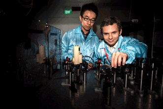
Researchers at the Centre for Disruptive Photonic Technologies at Nanyang Technological University in Singapore are working to advance metamaterials and nanophotonics. Photo courtesy of NTU, Singapore.
Despite the exciting potential for nanophotonics-based technologies, some major hurdles remain. For example, a major challenge is to develop a binary optical switch that is faster and consumes less energy than a field-effect transistor. Such a switch will mean a brute-force competition with nanoelectronics on its playground.
However, as Zheludev points out, radically new approaches for handling and processing information could also give nanophotonics a cutting-edge advantage. For instance, at the Centre for Disruptive Photonic Technologies, a device known as the oracle is used to solve the hardest problems by mapping them on a photonic network that can be interrogated with optical pulses.
But broader challenges also remain – which affect the entire field of nanophotonics – from management of waste nanomaterials to the standardization of production protocols.
“The biggest challenge is to reliably and cheaply construct devices on the nanoscale,” said professor Jeremy Baumberg, director of the NanoPhotonics Centre at Cavendish Laboratory at the University of Cambridge in England. “We have massive top-down industries that deliver electronics, but these are rather unsuited to nanophotonics. Better is the assembly of protein machinery throughout every cell in the natural world, and we have no idea yet how to take advantage of these ideas to construct nanophotonics devices that build architectures on the nanoscale with a whole mix of different materials.”