Christoph Hertzler and Ute Gauger, Trumpf Laser- und Systemtechnik GmbH
When is a boundary actually reached? When is “small” so small that anything smaller is simply not possible? Today’s smartphones are a never-ending fountain of information: They allow us to compare prices in real time, network with friends and navigate unfamiliar areas, and they easily replace the digital camera. Tomorrow’s smartphone might be on your wrist, on the bridge of your nose, in your ear or even on your retina. In any case, it will be linked with and to the body, controlled by gestures and speech.
It sounds a bit like science fiction, but it is an emerging reality. To actually bring this vision of the future – now not so distant – to market, the chip at the heart of the smartphone will have to become even more powerful. And that will be possible only if its circuits can be made even smaller.
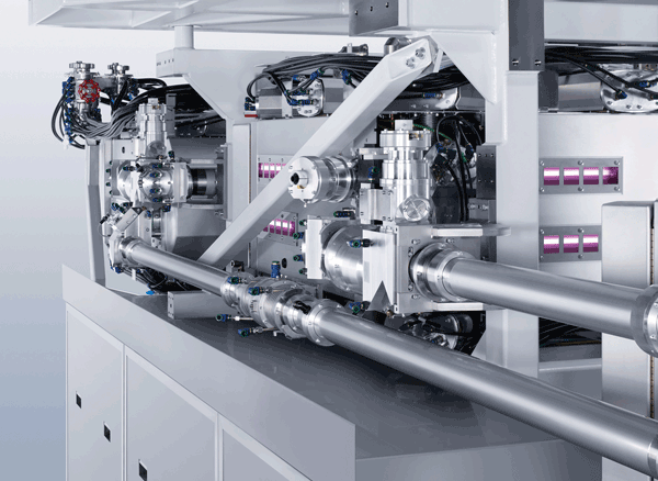 The relay optics and beam tubes are shown on these power amplifiers.
Frequently quoted in this context is Gordon Moore. Co-founder of Intel, the world’s leader in semiconductors, he realized as early as 1965 that the number of transistors on a given surface area of a chip would double every 18 months. Even today, Moore’s law continues to drive the industry, which is waging a battle – costing billions of dollars – for every square nanometer on the chip. But to pack ever more transistors on the semiconductors inside the chip sets, we need, in plain and simple terms, more light.
10 billion transistors on a chip
A microchip is born in the light of a photolithography machine. There, the miniaturized image of a circuit is projected onto a silicon wafer, exposing a photo-resist layer. Abbe’s resolution limit dictates that a light source cannot replicate any structure smaller than its own wavelength. This boundary is not insurmountable, however. At the present time, lithography units work with a wavelength of 193 nm but generate structures 22 nm in size and thus achieve performance well beyond this resolution limit. This is done with a variety of tricks and gimmicks.
However, the light sources now in use are, slowly but surely, approaching the limits of technical feasibility. It was more than 15 years ago that the semiconductor industry called the EUV Lithography Project into being, with the intention of engraving the tiniest of structures on the various levels of the microchip.
The objective of the project was to develop a stable source for extreme ultraviolet light (EUV) with a wavelength of 13.5 nm. This was because – with the assistance of this technology – it would be possible to produce structures less than 10 nm in size. This means, in turn, that more than 10 billion transistors could fit on a single microchip.
Flashes of light in a vacuum
But it’s not all quite so simple. The greatest challenge in EUV lithography is to generate light at just this 13.5-nm wavelength. The EUV source has to reach several hundred watts of power and make it available for further processing within the optical system. Plasma sources have proved to be the only solution available to date. Plasma is generated either by focusing high-intensity laser radiation or with high-energy discharges; tin and xenon are suitable as the input materials.
Laser-produced plasma has established a lead here. The idea behind this process sounds quite simple at first. A generator shoots tin droplets with 50 kHz into a vacuum chamber while a laser pulse impacts those droplets as they speed by. The laser thus strikes 50,000 tin droplets per second. The tin atoms are ionized, and a high-intensity plasma is created. A collector, using a multireflection configuration, catches the EUV light emitted by the plasma, focuses it and ultimately transfers it to the lithography system to expose the substrate.
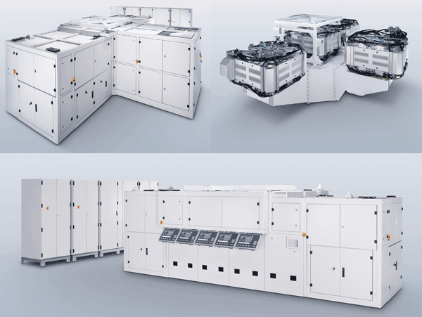
 This drive laser system from Trumpf includes control cabinets and radio-frequency generator cabinets.
The laser pulse for this purpose is delivered by a pulse-type CO2 laser system – the Trumpf laser amplifier. This system is based on the technology used for the continuous-wave CO2 laser and operates in a performance range exceeding 10 kW. In five amplifier stages, it boosts a CO2 laser pulse of just a few watts of mean power more than 10,000 times, outputting more than 30 kW of mean pulse power. Pulse peak power, however, can reach several megawatts.
To achieve perfect results, the laser pulse has to strike the tin droplet across as broad an area as possible. With its diameter of just 20 µm, the tin droplet is smaller than the laser’s focus spot. Consequently, the laser cannot transfer its full 30 kW of power to the tin droplet. To achieve this, the laser amplifier employs a clever ruse: It emits a pre-pulse and a main pulse, at slightly differing wavelengths, one immediately after the other. The pre-pulse strikes the tin droplet at initial laser power of 3 kW; the tin atoms ionize, and the plasma thus created expands. The main pulse, following close behind, strikes the plasma cloud, now expanded to about 200 µm in diameter, with 27 kW of pulse power.
Wavelength selected with care
There are two reasons for the selection of the 13.5-nm wavelength. First, at this wavelength the source beam exhibits intense lines, which means that the radiation output is especially high. This is because, at this wavelength, the lines in tin plasma are very strong. It is important to remember that plasma radiates discrete lines. Second, only the 13.5-nm wavelength makes it possible to manufacture the layer systems required for optical imaging at sufficiently high reflectivity. Refractive optical elements – such as lenses – absorb this wavelength. That is why EUV systems work exclusively with mirrored optical elements. The very short wavelength is also the reason why the entire process has to take place in a vacuum, since air would also absorb the EUV radiation.
 The Trumpf laser amplifier is based on the technology used for the continuous-wave CO2 laser and operates in a performance range exceeding 10 kW.
Anyone searching for an alternative to the demanding technology associated with EUV lithography will find that there really isn’t one. The optimization of previous technology, based on a laser beam with a 193-nm wavelength, has made it possible to image even smaller structures when exposing the substrate. This is done, for instance, by multiple exposure – double patterning – where each exposure step is carried out twice. Another option is immersion, whereby the higher refractive index of water is utilized.
In the meantime, it is possible, using conventional procedures, to create structures as small as 14 nm – which also represents the economical boundary. This means that, for the semiconductor industry, laser-supported EUV photolithography will continue to be the only way to create even smaller structures – and thus attain even higher performance for the chips.
The goal is within reach
The groundwork for this future has been laid. Since the beginning of 2014, third-generation laser systems have been delivered to manufacturers of photolithography systems, and the pre-pulse/main-pulse technology has become a standard feature. Right now, using these systems and the 13.8-nm wavelength, developers are producing the tiniest of structures. This means that today’s EUV source achieves a stable power output of between 30 and 40 W, while in the laboratory, peak values are currently at 70 W.
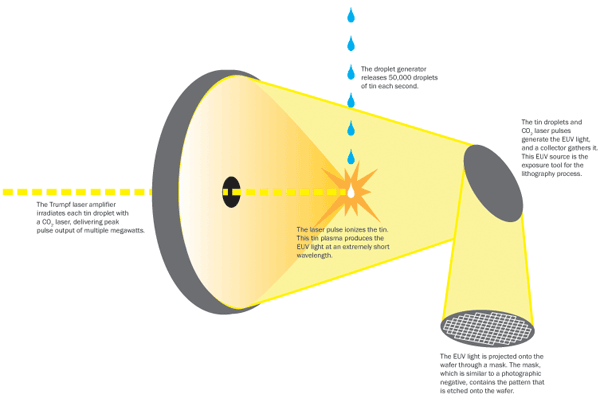 The laser-produced plasma process.
The whole thing will become economical and productive only at 250 W, however, and the developers have set 125 W as the next intermediate goal. To achieve this, they are fine-tuning systems, modifying parameters, beefing up the power of the CO2 laser and optimizing pulse lengths. Even now, several lithography systems are running in test production operations. In continuous use, they will deliver high quality and hold to their promise.
By the end of 2015, Trumpf aims to achieve the 250 W of optical power required for mass production. Then, at the latest, chip makers should be able to ready their latest generation of microchips for production with EUV lithography. This means that structures in even lower, single-digit nanometer ranges are drawing ever closer.
And once we’ve done that, we still will not have reached the end of miniaturization. That is why we want to postpone answering the question as to when “small” is the smallest possible.
Meet the author
Christoph Hertzler is the director of development for EUV systems at Trumpf Laser- und Systemtechnik GmbH in
Ditzingen, Germany; email: [email protected]. Ute Gauger is the company’s project manager for EUV systems; email: [email protected].