
Conquering the Silicon Photonics Production Bottleneck
Alignments for silicon photonics had been slow and sequential, but new fast multichannel photon alignment systems are yielding breakthroughs in parallelism, scalability and speed.
SCOTT JORDAN, PI
The first computer link using optical fibers was commissioned four decades ago to safeguard communications at the Cheyenne Mountain strategic command center1. We have since seen broad adoption of photonic communications in an unfolding trend of diminishing scale. Transoceanic fiber cables have replaced satellite links; photonic communications have become the backbone of transcontinental communications and serve as the foundation for regional and metropolitan communications, delivering bandwidth to business, consumers and homes.
Today, optical communications are a scalable and high-capacity mechanism for ever-shortening data links between data centers, racks, servers, cards and, soon, from chip to chip. IBM has even predicted a future chip architecture with hundreds of cores all interlinked by an on-chip optical mesh2.
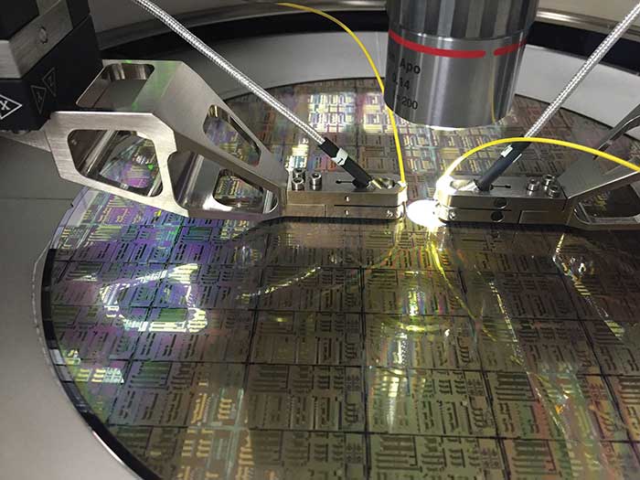
The rapid march of advances was interrupted by the industry dieback in the early 2000s as overcapacity and an economically unsustainable glut of under-differentiated ventures combined to winnow the field3. In hindsight, this bow to “photonomics” seemed inevitable4 as supply and demand found themselves catastrophically imbalanced. It meant for a quiet decade and a half, but only from a commercial sense. Technologically, the steady down-drop in scale continued in research and industrial laboratories, with the eventual goal being the elimination of copper as the default interconnect. With copper’s demise came the promise of bounties of capacity, throughput, parallelism, scalability and energy savings.
In 2002 — the year of the telecom meltdown — no one was talking about streaming media, social networks, big data or the Internet of Things. But as new wonders became fixtures of everyday life over the past decade, as waves of creative destruction washed away entire industries, bandwidth demand proceeded along an exponentiating path. Then, about five years ago, the semiconductor industry began driving photonics, motivated by the world’s appetite for data. And eventually, the photonics industry came back.
Alignment proves daunting
Testing and packaging a photonic device once meant attaching a single optical fiber to a single emitter or detector. Even this posed significant challenges. Photonic couplings approximate a Gaussian cross section. For transverse misalignments of two parallel circular optical waveguides of waist radii w1 and w2, this equates to a transmission T that diminishes with lateral misalignment d (classical Gaussian coupling)5.
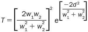
In the common case where w1 ≈ w2 , a misalignment of half a waist radius results in a reduction of throughput by 1 dB; misalignment of a full radius chokes coupling by a whopping 4 dB. The steep slope of the Gaussian means drift and other misalignment processes start bad and get worse. Multimode couplings are not necessarily easier to align, since their globally optimum orientation is less obvious.
In the late 1980s came the first alignment engines: the Nanotrak from Photon Control and the FX-1000 from Newport Corp. Both aligned single-mode fibers to devices, and the Launchmaster from York automated free-space coupling into a fiber or other device. These not only reduced the fiddly chore of transverse single-mode alignment to under a few seconds, they could maintain optimization in the face of drifts and disturbances.
These largely analog instruments employed a gradient ascent technique based on dithering one element in a small circle with respect to the other. A detector observed the resulting cyclic variation of coupled intensity. A phase demodulator derived the phase angle between the dither and the intensity signal, indicating the direction along the gradient. The amplitude of the modulation represented the magnitude of the local gradient, providing a measure of lateral misalignment. Between the phase and magnitude information (Figure 1), a servo could optimize and maintain the orientation of the devices. This technique could align even the then-new single-mode fibers.
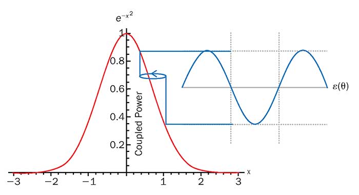
Figure 1. A graphical depiction of gradient determination via a circular dither, which modulates the coupled power observed at the photodetector. The phase of the modulation with respect to the dither indicates the direction toward maximum while its amplitude falls to 0 at optimum. Courtesy of PI.
Early mechanisms tended to be fragile, offer limited range and operate without position feedback, making them less than optimal for production purposes. These drawbacks began to be addressed with digital gradient search technology that originated in Newport’s AutoAlign system and subsequently acquired and further developed by ficonTEC. The first digital implementation of a gradient search, it was based on robust, industrial-class precision motion hardware capable of travels of many millimeters, driven by efficient software. It was quickly implemented into a host of packaging system designs suitable for 24/7 production applications. It utilized a point-wise dither followed by a gradient calculation and a corrective motion6. Observing Imin and Imax among the acquired dither points allowed estimation of the gradient |ε(θ)| as a measure of alignment error.

The corrective motion used the step size scaled to the error signal |ε(θ)| and subjected to limits to prevent overshoot. The process was then repeated. As ∇I→0 (the condition of alignment) the system naturally stopped when optimized, or it could align continuously.
PI implemented a novel piezo stepping mechanism to achieve similar aims, and in 1997 introduced a photonics alignment hexapod, a micro-robot that implemented hill-climbing algorithms and scans in firmware and could perform alignments and precision closed-loop motions in six degrees of freedom, with rotations cast by software to any desired center point, such as a focal point. This proved important for the packaging applications in the industry’s great blossoming and subsequent decline. Then came silicon photonics.
Silicon photonics is different
In silicon photonics (SiP), optical devices are fabricated on wafers in ways familiar from semiconductor microlithography. The devices are formed in layered fashion on the surface of a silicon substrate. The resulting waveguides present very different physics than the cylindrically symmetric geometries familiar from single-mode fiber applications. Characteristic dimensions can also be much smaller than what was typical in 2002. Often, diffractive couplers are used to kick light out of the wafer plane, making in-wafer devices accessible without dicing and facilitating some packaging approaches for the final devices. It’s common to see coupling cross sections that have a narrow, knife-edge profile in one dimension and a much broader profile in the orthogonal dimension. And the N inputs and M outputs of short devices can interact, with slight changes of alignment position at each of the inputs potentially steering the aligned position at the outputs, thereby making alignment a moving target.
The dimensions, profiles and inter-channel behavior are problematic for legacy alignment systems, which require a time-consuming looping sequence until a consensus alignment is achieved. Add the angular optimization required of arrayed devices and others, and the alignment times increase prohibitively.
All this posed obstacles for scalable packaging of SiP devices. And of course the most compelling reason to pursue silicon photonics is the ability to stamp out hundreds or thousands of devices in one go on a single wafer.
A realization emerged about the implications for wafer-level testing of photonic elements. As costly as a patterned wafer is — and it can exceed several million dollars — it represents a small fraction of its fully packaged devices’ value7. It is imperative that only known-good devices proceed to the packaging phase.
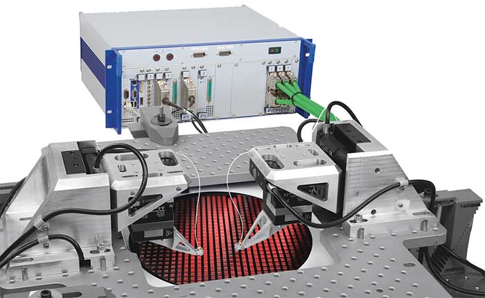
Figure 2. A fast multichannel photon alignment (FMPA) system for double-sided probing of on-wafer waveguide devices. Fully digital and closed-loop, it implements exclusion-zone capability, an internal data recorder, nanoscale-stable position-hold, and firmware-based fast scanning, modeling and multichannel N × M gradient search capability. Courtesy of PI.
Conventionally, electronic testing is routinely performed on wafers. An entire ecosystem of wafer-probing tools exists to support this in both the lab and fab. Wafers are contacted by an array of electronic probes; probe placement tolerances can be as tight as 20 to 30 μm today. Testing proceeds using a variety of stimuli, often at varying temperatures. In this way, each die is qualified and graded (binned) so that its status is known long before dicing.
Optical probing presents new complications: Coupling tends to be noncontact. Tolerances are two orders of magnitude tighter, placing extreme demands on probing system structural rigidity and stability. Furthermore, the value and fragility of a fully patterned wafer eliminates the use of open-loop motion devices — or should, in theory. Only closed-loop devices with real-time position encoding and a soft-limit (exclusion zone) capability should be allowed to operate within microns of a costly patterned wafer. Precision sensors also ensure that when alignment concludes, positions are held to nanometer-scale stabilities.
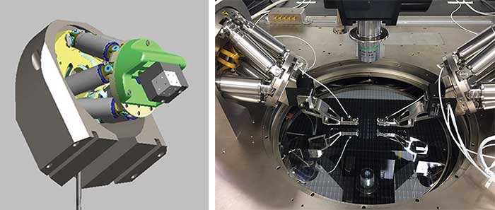
Figure 3. FMPA 6-axis packaging configuration utilizes a hexapod for long travel precision alignment and an XYZ piezo flexure nanopositioning scanner for fast fine alignment and tracking (left). FMPA 6-axis double-sided wafer probing configuration (right). Courtesy of PI.
The impasse posed by the mushrooming number of devices was only recently broken. First, the foundational point-wise gradient search was supplanted in the mid-2000s by a mathematically related but nonstop digital gradient search, an innovation8 that combined a continuous dither with synchronous observation of position and coupled power, enabling on-the-fly optimization at much higher speeds. This, in turn, yielded the newest development in alignment (Figures 2,3), called fast multichannel photon alignment (FMPA), a firmware-based, digital approach that provides alignment of multiple inputs and outputs and degrees of freedom, and can do so all at once, as it offers inherent parallelism9. The technique is also applicable to fast, parallel multi-degree-of-freedom alignment of reflective and refractive elements.
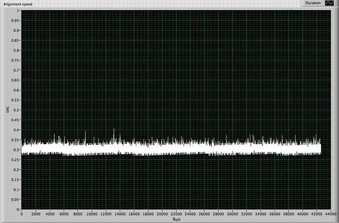
Figure 4. Time series of coupling recovery times from >40,000 random offsets of amplitudes and statistical distribution representative of wafer-prober placement errors. Courtesy of PI.
Implementing for speed
This capability can be built into the firmware of the alignment controller, along with areal and first-light scans, providing a significant multiplier of execution speed versus software-driven approaches. Software complexity can be reduced to issuing single commands to commence multi-channel, multi-degree-of-freedom global optimization.
Execution of the firmware-based alignment commands is straightforward and fast. Users can define the alignment or scan process by specifying its operational parameters, such as which axes and which optical metrology inputs to optimize. Typical transverse optimizations are complete in about 250 to 400 msec (Figure 4). All told, global input/output SiP-device alignment is about two orders of magnitude faster than legacy techniques applied sequentially.
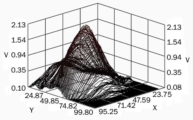
Figure 5. Fast sinusoidal raster scan showing departure from a classical Gaussian coupling cross section. Messy profiles of this sort cannot be reliably optimized with traditional alignment algorithms. Courtesy of PI.
Of course, rather than completing when a satisfaction criterion is reached, any process or processes can be configured to continue or restart, maintaining global alignment against drift and other disturbances — which is essential for devices incorporating active electronic elements such as lasers or heaters. When halted, the device remains under nanostable closed-loop position control.
Fast profiling
Alignment speed can be limited by mechanical and computational issues. Mechanical oscillations are suppressed by motion patterns engineered for minimal vibration: a sinusoidal raster and single-frequency or constant-velocity spirals. Running the search algorithms and optical feedback inside the controller firmware reduces execution time compared to traditional software-based methods implemented on a host computer. Additional throughput can be gained by increasing the piezo-driven scanning area and improving responsiveness of the mechanisms. A parallel-kinematics approach allows the reduction of the moved masses and thus higher acceleration over larger motion ranges than previously available with serial kinematics designs. Closed-loop control eliminates drift and positional uncertainty that restrain the accuracy of open-loop nanopositioners often deployed in lab-class alignment applications. The sinusoidal raster is similar to a conventional serpentine scan, but with bidirectional data acquisition for speed and without the vibration-inducing stop/start at the beginning and end of each scan-line. Typical full-field scans are complete within 200 to 400 msec (Figure 5).
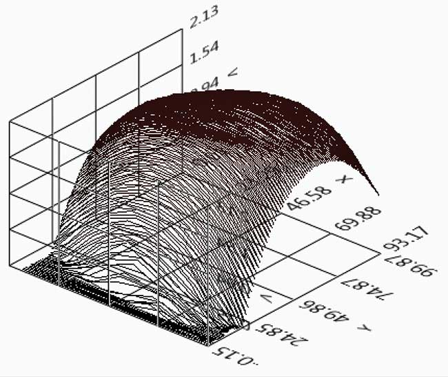
Figure 6. Top-hat coupling, typical of detector alignment and DMD testing. The FMPA controller can automatically determine the position of the centroid. Top-hat couplings could not be aligned by any integrated alignment technology prior to FMPA. Courtesy of PI.
Circular scan patterns are more ideal for sensitive opto-mechanical situations of limited clearance and tend to be even faster than sinusoidal scans. Fast, high-resolution profiling of components is achieved by controllers with internal data recorders capable of synchronous, simultaneous acquisition of multi-axis position and optical power at data rates up to 20 ksamples/s.
Areal scans can supplement built-in modeling capability to accurately calculate the optimum position using sparse (that is, fast) scans; the modeling calculations themselves complete in typically under 1 ms. Modeling is also integrated for flat-topped (top-hat) couplings, when a comparatively large-area element is probed by a fiber of small core dimension (Figure 6).
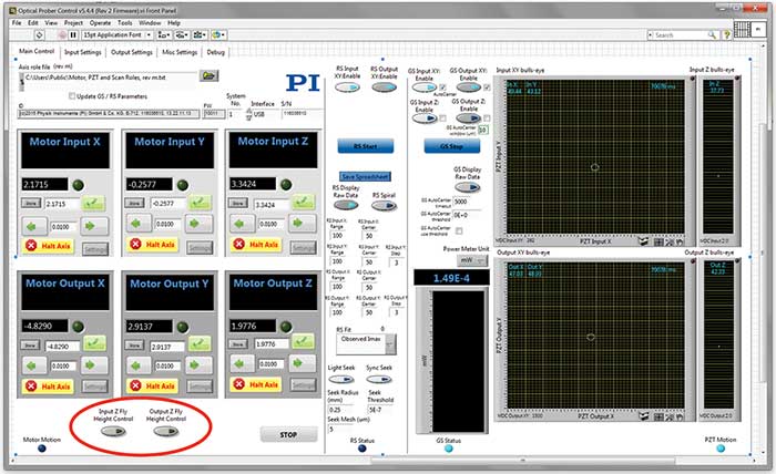
Figure 7. This graphic user interface example provides intuitive access to key FMPA functionality. Shown: double-sided XYZ waveguide alignment and novel cap-sensor-enabled fly-height control (circled). Courtesy of PI.
Often a hybrid strategy is ideal: Perform an areal scan to quickly localize the approximate position of each coupling’s optimum, then command the gradient search to align all the couplings and degrees of freedom in parallel to achieve the consensus optimum.
Fast multichannel photon alignment represents a break from the past in ways relevant to silicon photonics. Previously, alignments were sequential and slow and software-intensive. With FMPA, they are parallel and fast and firmware-implemented. This yields scalability. Up to six degrees of freedom are supported per coupling. Fast, fab-class interfaces speed communications, with network-compatibility for integration into production information systems. For rapid application development and supportability, a mnemonic command set provides deep functionality for alignment and precision motion and is supported by dynamic libraries (.dll for Windows, .dylib for macOS, .so for Linux) and libraries for LabVIEW, MATLAB, Python and other popular architectures. These allow quick construction of applications, such as a graphical interface (Figure 7) that is locally or remotely scriptable by Python, MATLAB and other text-executive environments.
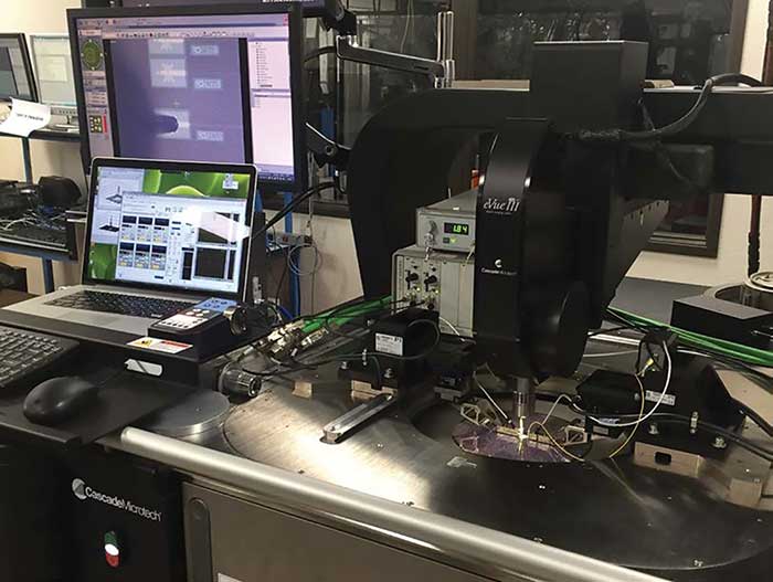
Figure 8. Cascade Microtech’s pioneering CM300 photonics-enabled engineering wafer prober integrates PI’s Fast Multichannel Photonics Alignment systems for high-throughput, wafer-safe, nano-precision optical probing of on-wafer silicon photonic devices. Courtesy of Cascade Microtech, division of FormFactor Inc.
FMPA is available to engineers, researchers and OEMs (Figure 8) and is built into packaging and probing tools from some of the most respected integrators in the industry.
Meet the author
Scott Jordan is head of photonics for PI, and a PI Fellow. A physicist with an MBA in Finance/New Ventures, he has multiple contributions to alignment automation.
References
1. I. Lee, ed. (2009). Handbook of Research on Telecommunications Planning and Management for Business. Hershey, Pa.: IGI Global.
2. IBM (March 2008). IBM researchers develop world’s tiniest nanophotonic switch to route optical data between cores in future computer chips. www-03.ibm.com/press/us/en/pressrelease/23700.wss.
3. S. Jordan (2002). Photonomics: Automation approaches yeld economic aikido for photonics device manufacture. Proc SPIE, Vol. 4771, pp. 49-60.
4. S. Jordan (January 2001). The Coming Economic Crunch in Photonics … and What You Can Do About it. Presented at Automation in Photonics, Information Gatekeepers Inc.
5. R. Boudreau and S. Boudreau, eds. (2005). Passive Micro-Optical Alignment Methods. Boca Raton, Fla.: CRC Press.
6. S. Jordan. Throughput maximizing systems for substantially unimodal throughput profiles. U.S. Patent 5278934. Filed March 18, 1991, issued January 11, 1994.
7. W. Van Parys (2009). Optimization of an Integrated Optical Isolator Based on a Semiconductor Amplifier with a Ferromagnetic Metal Contact. University of Ghent.
8. S. Jordan. Aligning apparatus and method using on-the-fly determination of throughput-profile gradient for current positioning of radiated influence supplier and/or receiver. U.S. Patent 7236680. Filed August 16, 2004, issued June 26, 2007.
9. PI (Physik Instrumente) LP (February 2017). Parallelism in Photonics Alignment Automation: Key to Economic Test & Packaging.
/Buyers_Guide/PI_Physik_Instrumente_LP_Motion_Control_Air/c11819