Photonics Handbook
Silicon-on-Insulator Substrates: The Basis of Silicon Photonics
With the advancement of mobile technology and applications, better internet and data connectivity is increasingly in high demand. Silicon photonics has the potential to become the key technology.
ARNAUD RIGNY, SOITEC
The demand for greater internet connectivity is driven by mobile device applications, new video-on-demand services and connected industrial services. And it’s growing at an average rate of 24 percent per year (Figure 1). All of this internet traffic flows through large data centers where information is stored and computed. A typical data center consists of several hundred thousand servers interconnected by optical cables covering distances of several kilometers inside a building. The speed of connectivity within data centers is gradually increasing, as reflected by the connectivity standard evolution and particularly the ethernet standard.
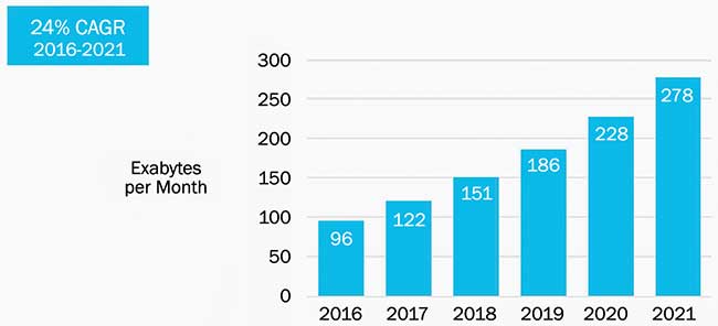
Figure 1. The demand for greater internet connectivity is increasing at an average rate of 24 percent per year. Courtesy of Soitec.
This connectivity was 40 Gbps in 2010 and 100 Gbps in 2015; there is a roadmap to reach 200 Gbps by 2019 and 400 Gbps by 2022 (Figure 2). To achieve these levels of data rate transfer, optical technology is widely used and is of choice for distances of more than 100 m. Optical communication uses optical fiber as a transmission medium, but fiber optics requires more and more optical components, such as lasers, modulators and multiplexers, to run in parallel.
This puts optical connectivity at the heart of data center challenges. So what optical technology will achieve the required performance while also staying within an acceptable energy budget and an acceptable cost?
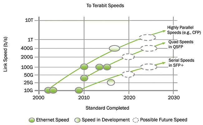
Figure 2. Ethernet connectivity is expected to grow from 40 Gbps in 2010 to 400 Gbps by 2022. Courtesy of Soitec.
Optical communication uses optical fiber as a transmission medium. At each end of the fiber, a transceiver emits and receives light and encodes the luminous flux. Optical fibers can be either multimode fibers (MMF), which ease light coupling within the fiber but limit the transmission distance, or single-mode fibers (SMF), which allow long-distance transmissions for applications such as telecommunications. To make transmissions efficient, five wavelength bands have been defined that exhibit the lowest attenuation — an 850-nm band, band O (around 1.3 μm) and bands S, C and L (each around 1.55 μm). Because of optical transmission properties, MMF is used for the 850-nm band and SMF for bands O, S, C and L.
The light sources are manufactured with direct-gap, III-V semiconductor materials; using silicon and germanium is not possible. Typically, GaAs is used for wavelengths of 850 nm and InP for wavelengths of 1.3 μm and 1.55 μm.
Common optical transceivers for data communications are composed of a directly modulated light source (on/off) and a fiber-coupling optical system. These are packaged in a hybrid way, meaning that each component (laser, lens, etc.) is individually packaged and assembled. This approach faces severe challenges in terms of cost and scalability as transceiver performance increases.
SOI substrates
As the bit rate within data centers increases from 10 to 400 Gbps, transceivers must become more complex. In particular, laser direct modulation is limited to 25 Gbps because of low frequency response, making multilevel external modulation mandatory. New generations of transceivers are integrating several light sources and external modulators for more efficient modulation and wavelength multiplexers to combine several light streams into the same fiber. This roadmap is not compatible with current hybrid technology, which consists of free space assembly of optical components. Therefore, an integration platform is needed to give optical functions greater power efficiency, lower costs and high-volume production.
Silicon photonics addresses this problem by integrating optical components on a silicon platform that leverages the existing CMOS ecosystem, including front-end and back-end processes. Furthermore, silicon is a transparent material with wavelengths of 1.3 μm and 1.55 μm, and is therefore particularly compatible with InP lasers and SMF fibers.
The integration platform consists of components using light waveguides made on a silicon substrate. This allows the guided light to undergo the necessary optical treatments such as modulation or filtering. But it is almost impossible to have an optical waveguide with acceptable performance (low propagation loss, etc.) on a silicon substrate without special layers. This is where silicon-on-insulator (SOI) substrates come in.
An optical guide, such as optical fiber, is made of transparent optical material (pure silica in the case of fiber) with a high refractive index (the core) surrounded by a material (silica doped in the case of fiber) of lower refractive index (Figure 3). Thus, the light is confined by reflections at the interface of the two materials.
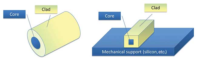
Figure 3. Optical fiber is made of pure silica with a high refractive index and surrounded by a material of lower refractive index, confining the light reflections at the interface of the two materials. Courtesy of Soitec.
The principle is the same for silicon, as its core is monocrystalline silicon (not to attenuate the light) surrounded by silicon oxide of much lower refractive index. But to make guides on a planar wafer surface, it is necessary to create a layer stack using a silicon wafer (mechanical support), silicon oxide (clad) and monocrystalline silicon (core). The waveguide is then made by etching the silicon where an optical guide is desired and depositing silicon oxide afterward. The SOI wafer includes a layer of silicon, a buried oxide (BOx) and a wafer support (Figure 4).
With guided optics, passive components such as splitters, mode adapters or wavelength multiplexer filters can then be easily made.
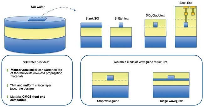
Figure 4. The core is monocrystalline silicon (not to attenuate the light) surrounded by silicon oxide of much lower refractive index. Courtesy of Soitec.
Thanks to the semiconductor property of silicon, it is also possible to create active components whose functionality is electrically controlled, such as a modulator. This is done by doping a PN junction in the optical guide, thus controlling the optical index of the guide. In this way, Mach-Zehnder modulators are designed (Figure 5). By splitting light in two different paths and applying a phase delay in one arm through the PN junction, constructive or destructive interference can be created when recombining the two paths. This allows the amplitude of the light output to be electrically controlled.
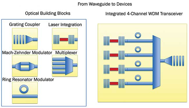
Figure 5. The semiconductor property of silicon allows creation of active components whose functionality is electrically controlled, such as a modulator. Courtesy of Soitec.
To make optical components that process the signal and are compatible with the coupling of a SMF fiber, the guides themselves must be single mode. This constraint imposes typical dimensions on the order of 2 µm for the silicon oxide layer and 0.2 µm for the monocrystalline silicon layer. Thus, to create optical components on a silicon platform, the starting wafer must typically have the following structure: 0.2 μm Si/2 μm BOx/Si wafer handle.
SOI in silicon photonics
In creating the silicon oxide layer, the technology that produces the best quality is the oxidation of a silicon wafer. The difficulty lies in producing a thin monocrystalline layer on oxide. Neither epitaxy nor pSi deposition and recrystallization can be used because SiO2 is not crystalline. The stack can be made by bonding a second silicon wafer and thinning — a process known as BSOI. However, this limits silicon layers to thicknesses of 3 µm or more.
The key technology to realize thin-silicon SOI wafers is called Smart Cut, which was invented at CEA-Leti and is manufactured by Soitec. Silicon photonics research and development groups have widely used Smart Cut technology (Figure 6) to industrially manufacture SOI wafer structures. Today, such wafers are widely used in power, radio frequency and CMOS components.
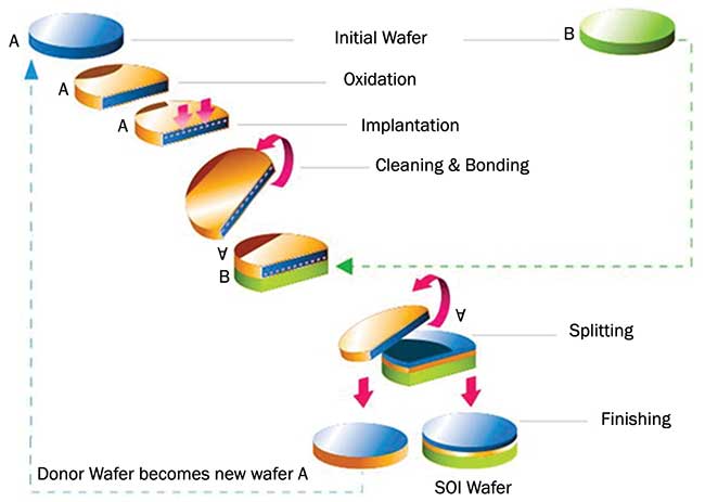
Figure 6. Depiction of Smart Cut technology, manufactured by Soitec. Courtesy of Soitec.
A silicon wafer is oxidized to produce a thermal oxide layer. A second wafer is then implanted with H+ ions where the implantation depth is controlled by the ion dose and energy — this depth is typically on the order of a few nanometers to a few microns, depending on the need. After implantation, the two wafers are fused by molecular bonding, with the implanted zone on the side of the bonding interface. After heat treatment, the implanted substrate separates from the rest of the structure at the implantation depth of the H+ ions.
The result is a structure composed of a silicon wafer, an oxide layer and a thin monocrystalline silicon layer as well as another slightly thinner bulk silicon wafer.
The first structure is called an SOI wafer, while the second wafer can be reused in another Smart Cut process.
After a finishing step to cure the surface quality of the silicon layer, the complete SOI wafer has the following unique characteristics:
• Monocrystalline silicon layer on a thermal oxide layer.
• Layer thickness between a few nanometers and 1.5 μm.
• Uniformity that can be as low as +/− ?Å.
• Surface quality (roughness, defects, etc.) comparable to a bulk silicon wafer.
• Robust bonding interface compatible with high-temperature heat treatment (1200 °C) used in the CMOS process.
• Thermal oxide layer with a thickness of a few nanometers to a few microns.
• Wafer compatible with the CMOS front-end process.
To meet the needs of various applications, a range of products has been developed based on the thickness of silicon and BOx.
The uniformity of the silicon layer is a key parameter for optical components. Indeed, the processing of the optical signal mainly uses the phenomenon of interference between light waves. Thus, it is possible to make modulators by controlling constructive or destructive interferences, using coupler grating to connect the light coming from the fiber with the silicon chip and apply wavelength multiplexer filters. This interference phenomenon is very sensitive to the geometrical dimensions of the optical guides, in lateral dimension and thickness. The latter is directly related to the thickness and uniformity of the silicon layer on the SOI wafer.
Based on different studies evaluating the impact of SOI layer consistency on component performance and manufacturing efficiency, the industry needs uniformity between +/− 2 nm and +/− 3 nm (Figure 7). This is necessary across the whole wafer layer, but also from one wafer to another to obtain identical performance from all components. For a layer of 220 nm, the industry needs layer uniformity on the order of 1 to 2 perce
nt of the total thickness. The tolerance is similar to the distance between two silicon atoms in the crystal (i.e., 0.54 nm). This is a substantial technological challenge.
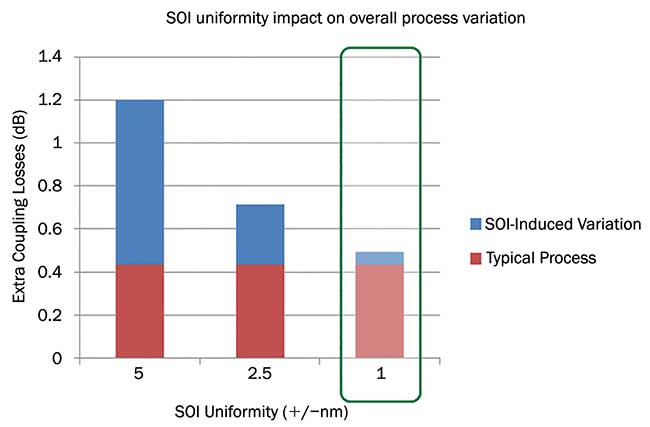
Figure 7. Based on the impact of SOI layer consistency on component performance and manufacturing efficiency, uniformity must be between +/− 2 nm and +/−3 nm. Courtesy of Soitec.
By using silicon photonics, optical components can achieve the faster data transmission rates needed to handle increasing internet traffic. Silicon technology used in the CMOS industry enables the integration of optics on a low-cost platform that can be manufactured in high volumes.
At the heart of silicon photonics is the SOI wafer, which makes it possible to integrate optics into silicon. Smart Cut technology is particularly well suited to industrially manufacture SOI wafers for photonics by creating a uniform (+/− 3 nm) silicon layer on silicon oxide of 2 µm (Figure 8).
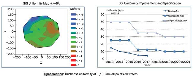
Figure 8. Mapping of the thickness obtained on an optimized wafer. Thickness accuracy equivalent to an atomic layer has been demonstrated and consistency of +/− 5Å has been measured. Courtesy of Soitec.
Thus, optical silicon technology will solve the challenges for the telecommunication and data communication industries. But optics is also a very powerful technology for other applications, including manufacturing gas sensors, biological sensors and laser detection, such as lidar. Looking ahead, there will be many opportunities to leverage silicon photonics in widely diverse fields including health care, smart cities and the automotive industry.
Meet the author
Arnaud Rigny is the business development manager for Soitec; email: [email protected].
/Buyers_Guide/Soitec/c13786