Cavities in photonic crystals can be used for creating optical logic gates, the building blocks for computing.
RENJU RAJAN, P. RAMESH BABU AND K. SENTHILNATHAN, VIT UNIVERSITY
When it comes to computing, one of the primary bottlenecks in increasing data transfer rates is the conversion time required from optics to electronics when the signal reaches a semiconductor microprocessor. One approach to addressing this problem would be converting systems to ones that are based on optics, with optical microprocessors in place of semiconductor microprocessors. Achieving this feat would lead to an era of all-optical information processing.
Optics, however, is not the sole technology eyed for the future of computing. Myriad technologies, known as quantum computing technologies, are also under consideration. Even though they lack some of the advantages of photonics, they have immense potential to overtake conventional systems.
Information processing in photonics is currently handled by artificial structures known as photonic crystals1. These dielectric structures can be made from materials such as silicon, compound semiconductors or polymers. The functionality of these structures depends on the periodic variation in refractive index, which results in photonic band gap in the structure at a particular frequency range.
Light localization
These structures, which reflect light in the forbidden frequency range, prohibit the light’s passage through it. Alternatively, if there is a defect in the periodic structure, such as a line defect that forms a waveguide or a point defect that creates a cavity, the forbidden frequencies can be confined within the structure with little propagation loss2. This phenomenon, known as light localization, was first predicted in 1987 and has come to fruition with photonic crystals3. A cavity created in a photonic crystal due to a point defect is illustrated in Figure 1.
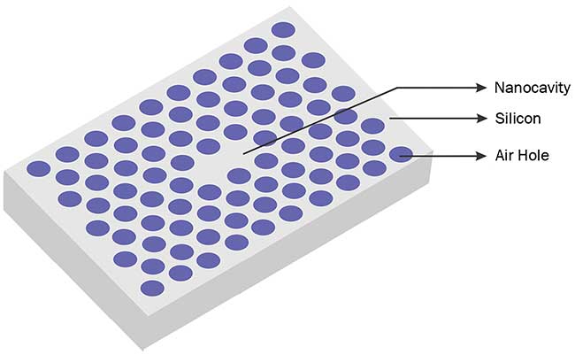
Figure 1. Cavity created in a photonic crystal slab. A cavity can be created in a photonic crystal by introducing the aperiodicity in the lattice. Courtesy of Renju Rajan.
Cavities in photonic crystals can be used for creating optical logic gates, the building blocks of computing. All arithmetic and logic operations are carried out in a computer making use of logic gates — a modern PC relies on them to perform tasks based on the program stored in its memory.
Once the technology for implementing logic gates is in place, it is a pretty straightforward process toward realizing an optical microprocessor. Among various logic gates, NAND and NOR are said to be universal gates since they can be used for performing all other logical operations. In other words, a combination of NOT along with AND or OR can be used for making all logical operations. Here, the implementation of NOT and OR gates using photonic crystals is covered.
In the near future, a proper combination of these gates can be used for designing an optical microprocessor.
Logic gates are computational elements that provide an output state based on their inputs. In semiconductor chips, logic gates are constructed with circuits that consist of transistors and diodes. The transistors have an inherent logical functionality; in other words, the logic gates provide an output that could be either 1 or 0 depending on their functionality. The input to the logic gates is usually a low or high voltage. In this way, the device can be used for generating binary digits. A logical switching can be carried out by transistors based on the input current or voltage values, which is the cornerstone of today’s semiconductor industry.
In optics, switching can be realized using optical cavities. An optical cavity supports only certain wavelengths depending on the length and refractive index of the cavity. More specifically, the length of the cavity should be an integral multiple of half the wavelength. This ensures that nodes are formed at both the ends of the cavity. Once the length of the cavity is fixed, its transfer properties depend on refractive index only. However, when the intensity of the light is sufficiently high, the refractive index depends on intensity of light, too. This phenomenon, known as the optical Kerr effect, can be harnessed for achieving optical switching with an optical cavity4. In this technique, a laser pulse is used to change the refractive index of the cavity medium, which, in turn, enables the system to switch to another logical state (Figure 2).
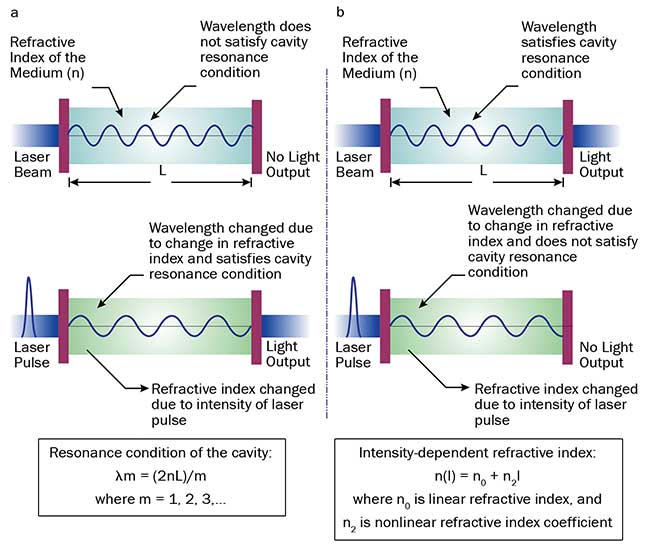
Figure 2. Optical switching process mediated by an optical cavity. A high-intensity laser pulse tunes the wavelength of light inside the cavity caused by changes in refractive index, and thereby satisfies the cavity resonance condition, allowing the laser beam to appear at the cavity output (a). A high-intensity laser pulse detunes the wavelength of light inside the cavity caused by change in refractive index, and thereby violates the cavity resonance condition, prohibiting the laser beam from appearing at the cavity output (b). Courtesy of Renju Rajan.
For realizing logic gates based on this technique, two types of cavity configurations can be used. The first configuration involves a cavity length set to have resonance wavelength below the wavelength of input light (Figure 2a). In the other configuration, the cavity length is set to have resonance wavelength at the wavelength of input light (Figure 2b). In the first case, the change in refractive index caused by the laser pulse tunes the input wavelength to match the resonance wavelength of the cavity. In the second case, the laser pulse causes the resonance wavelength to differ from the input wavelength, prohibiting the passage of light through the cavity. Both of these switching approaches can be put to good use for creating optical logic gates.
Logic gates using photonic crystals
The implementation of a NOT gate using a photonic crystal is considered first. For this purpose, the optical cavity considered here has a resonance wavelength the same as that of the incident light. This cavity is represented by S in Figure 3. The optical cavity serves as the coupling point between input and output waveguides. A bias light sent through the input waveguide is coupled with the optical cavity and crosses over to reach the output waveguide, as the resonance wavelength of the cavity is the same as that of the input light. On the other hand, when a laser pulse is sent along with the bias light, because of the high intensity of the laser, the refractive index of the cavity medium is altered, prohibiting the coupling of light into the output waveguide. This scheme is useful for realizing a NOT gate. Here, the presence of a laser pulse denotes a logical one state at the input waveguide. Because of the change in refractive index of the cavity, this laser pulse detunes the resonance wavelength away from the resonance condition and hence the output turns logical zero. But in the absence of a laser pulse that denotes a logical zero state at the input, the coupling is effective, and the light reaches the output waveguide representing a logical one state. This circuit that satisfies the NOT logical operations can be used for creating a NOT gate (Figure 3).
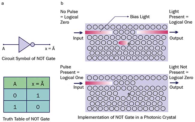
Figure 3. Circuit symbol and truth table of a NOT gate (a). Implementation of NOT logical operation using an optical microcavity in a photonic crystal slab (b). Courtesy of Renju Rajan.
The operation of an OR gate using photonic crystals is considered next. The circuit for realizing this gate consists of three optical cavities: Two of them are coupled to input waveguides; the third one acts as the coupling point between input and output waveguides and is also coupled to both of these cavities. The cavities, L, coupled to input waveguides have resonance wavelength lower than that of the bias light (Figure 4b). Conversely, the third cavity, S, coupled to output waveguide has resonance wavelength set to be the same as that of the bias light. The bias light from the input waveguides cannot traverse the cavity since its wavelength does not match the resonance wavelength of the cavity. This constraint can be sorted out by sending a high-intensity laser pulse that enables the cavity to achieve resonance with the wavelength of bias light because of the change in refractive index of the cavity medium. In this way, the high-intensity laser pulse enables the cavity to open up for the bias light.
The presence of a laser pulse at the input waveguide denotes a logical one state, whereas its absence denotes a logical zero. Once the bias light reaches any of the two intermediate cavities, it will be coupled to the third cavity, which has a resonance wavelength the same as that of the bias light. Subsequently, the bias light will reach the output waveguide by its coupling with the third cavity.
The presence of light at the output waveguide denotes a logical one state, whereas its absence denotes a logical zero state. In this way, the circuit with three optical cavities can effectively execute OR logical operations for realizing an OR gate (Figure 4).
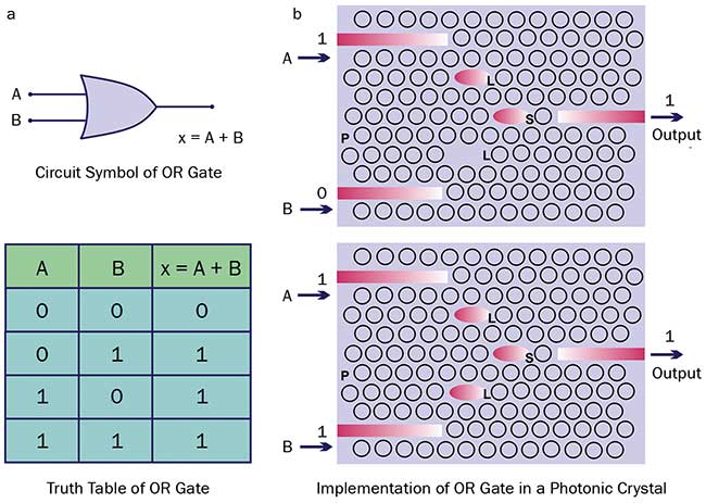
Figure 4. Circuit symbol and truth table of OR gate (a). Implementation of NOT logical operation using optical microcavities in a photonic crystal slab (b). Courtesy of Renju Rajan.
It is possible to realize the universal gate NOR by combining the NOT and OR gates. Further, an AND gate can be derived from a proper combination of NOR gates, as practiced in digital circuitry5. This makes it possible to realize an optical microprocessor using photonic crystals.
The advancement of photonic crystals in optical computing would give an impetus for further venturing into the arena of quantum computing.
The availability of high-quality-factor optical cavities and coherent light sources such as lasers makes photonics an appealing platform for this paradigm shift in computation.
From a technological point of view, it is better to adopt quantum computing in photonics at an early stage in order to avoid performance impasses that can hinder a conventional system. As a fundamental particle that gave birth to the realm of quantum mechanics, the photon has a role to play in the design of future quantum computers.
Meet the authors
Renju Rajan is a Ph.D. candidate in physics at VIT University in Vellore, India. He holds bachelor and master of science degrees in physics from Mahatma Gandhi University, Kottayam. His areas of research include photonic crystals for information processing and Bose-Einstein condensation of photons; e-mail: [email protected].
P. Ramesh Babu is a professor of physics at VIT University, Vellore. He holds master of science, master of philosophy and Ph.D. degrees in physics from the University of Madras, Chennai. His areas of research include fiber Bragg gratings, optical fiber communications, photonic crystal fibers and pulse compression; e-mail: [email protected].
K. Senthilnathan is a professor of physics at VIT University, Vellore. He holds master of science and master of philosophy degrees in physics from the University of Madras and a Ph.D. from Anna University, Chennai. His areas of research include optical fibers, fiber Bragg gratings and photonic crystal fibers; e-mail: senthee@gmail. com.
References
1. E. Yablonovitch (2001). Photonic crystals: semiconductors of light. Sci Am, Vol. 285, Issue 6, pp. 46-55.
2. J.D. Joannopoulos et al. (1997). Photonic crystals: putting a new twist on light. Nature, Vol. 386, pp. 143-149.
3. M. Notomi (2010). Manipulating light with strongly modulated photonic crystals. Rep Prog Phys, Vol. 73, Issue 9, pp. 1-57.
4. P.N. Butcher and D. Cotter (1991). The Elements of Nonlinear Optics. Cambridge: Cambridge University Press.
5. R.J. Tocci et al. (2007). Digital Systems: Principles and Applications. 10th ed. Upper Saddle River, N.J.: Pearson Education.