Advancements in disordered nanophotonics and fabrication techniques could lead to enhanced photovoltaic cells.
GUILLAUME GOMARD, KARLSRUHE INSTITUTE OF TECHNOLOGY (KIT)
Recent reports forecast solar power will become the world’s cheapest form of energy within the decade. The dramatic decrease in the price of photovoltaic (PV) solar modules in recent years (now hovering around 31 cents per watt peak) has resulted from new advances in production — the price per module was scaled down by approximately 20 percent as production volume doubled.
On the performance side, there were continuous improvements in solar cell design. In particular, efficient light management solutions have been implemented to make better use of the incoming photons and to enhance the power conversion efficiency of PV devices. An example is surface texturing of wafer-based silicon solar cells, which results in an improved in-coupling of the light into the PV cells.
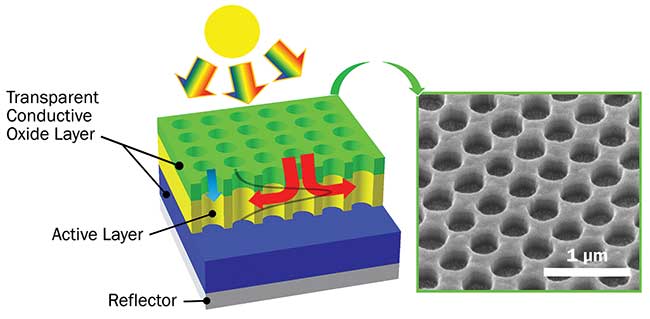
Thin-film solar cells with active layer patterned as 2D absorbing photonic crystals improve light in-coupling (light-channeling effect, see blue arrow) and enable control of the coupling of the incoming light with quasi-guided modes (light-trapping effect, see red arrows). Courtesy of Guillaume Gomard/KIT.
More advanced light-harvesting designs were employed to tackle the optical losses (incomplete sunlight absorption and reflection losses) taking place in devices based on thin absorbers. This is a cost-effective technology employing reduced absorber thicknesses (one to three orders of magnitude lower than for their wafer-based counterparts) and compatible with lower-grade materials.
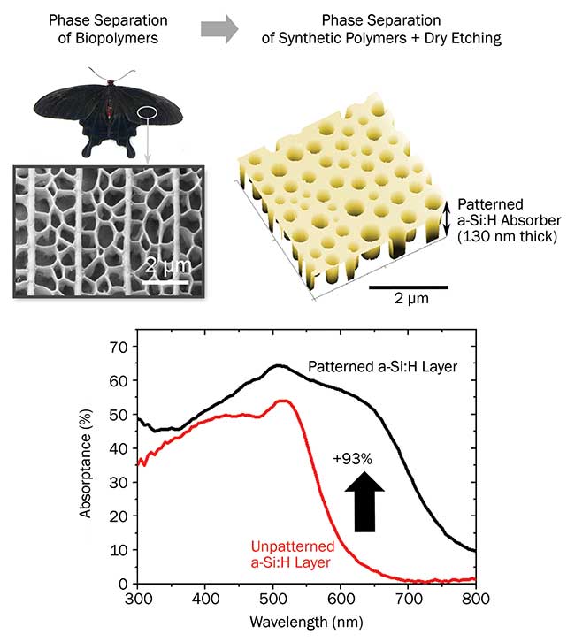
Enhanced sunlight absorption in nanopatterned thin absorbers inspired by the light-harvesting, disordered nanohole arrays decorating the black butterfly wings. (a-Si:H = hydrogenated amorphous silicon). Courtesy of Guillaume Gomard/KIT.
With the rise of nanofabrication techniques and powerful numerical simulation possibilities, many light-management strategies have been tested over the last 20 years in an attempt to enhance sunlight absorption in thin-film solar cells. Plasmonic, metamaterial, and dielectric light-scattering structures were all tested in lab-scale demonstrators in pursuit of this objective. Discussed here are the research efforts aimed at improving sunlight absorption by directly patterning the PV active layer, silicon. This topic, whose foundation dates back half a century, has attracted researchers from the nanophotonic and photovoltaic communities and beyond, with a common goal of introducing designs that satisfy the demanding solar cell optoelectrical requirements and that can be produced at reasonable costs.
Early days of light trapping
In 1969, Albert E. St. John patented an apparatus for improving IR light absorption in silicon detectors. His invention consisted of introducing a rough, sandblasted texture on the back side of the detector to randomize the angular distribution of the collected light and increase its optical path length, hence enhancing its absorption probability.
It is not surprising that this concept of “light trapping,” particularly relevant to harvesting the low-energy photons that were poorly absorbed in thin silicon layers, was applied to the PV technology as early as the 1970s. In addition to roughened, light-scattering rear surfaces, grooved mirrors were also proposed to induce total internal reflection of the collected light. This approach ensured an efficient absorption even in silicon layers with a thickness of only a few micrometers.
In the early 1980s, the idea of exploiting the easily adjustable light-diffraction properties of periodic gratings to achieve light trapping appeared in a patent and in scientific articles. Exact numerical calculations performed by Ping Sheng and colleagues demonstrated the potential of this concept by considering diffraction gratings formed in the rear mirror of hydrogenated amorphous silicon (a-Si:H) solar cells relying on submicrometer-thick absorbers1.
In this seminal work, the optical benefits of using periodic photonic structures — for example, the possibility of overcoming the absorptance obtained with a randomly roughened reflector in a desired spectral range — was highlighted along with their main limitation: wavelength selectivity.
These two counteracting effects have influenced recent developments of patterned PV absorbers designed to absorb sunlight over a broad angular and spectral range. This is desirable for solar cells harvesting the direct component of sunlight and the diffused one (scattered by clouds, reflected by surrounding surfaces) over a large bandwidth, typically extending over several hundreds of nanometers.
Patterned thin active layers
By optimizing the photon’s lifetime in the active layer, light-trapping structures can significantly enhance the absorptance near the band edge of the PV active material and, in turn, boost the generation of photocurrent. The light-trapping configurations related to structures placed in the vicinity of the absorbing layer discussed above were most often integrated in the rear side of the devices.
By optimizing the photon’s lifetime in the active layer, light-trapping structures can significantly enhance the absorptance near the band edge of the PV active material and, in turn, boost the generation of photocurrent.
An alternative route, followed by several research groups worldwide, consisted of directly patterning the PV active layer to form light-scattering elements that benefit from the high refractive index contrast between the absorber (refractive index around 3.5 in the case of crystalline silicon, c-Si, at a wavelength of 1.1 µm) and the ambient (only 1 and 1.5 for air and glass, respectively).
In this top-down approach, micro- and/or nanoholes are drilled into the absorber. Although the total absorbing volume is reduced after this etching step (by more than half in some cases), the overall integrated absorptance can still be significantly increased thanks to more favorable light-coupling conditions.
Here, two cases need to be distinguished by the thickness of the patterned absorber:
(1) When the patterning is only superficial and an optically thick absorbing layer lies below the surface corrugation, the etched micro-/nanoholes act as a diffraction grating. In this case, the path length can be increased by coupling the incoming light to high-order modes, ensuring large propagation angles within the absorber. An example of such a configuration would be a diffraction grating etched over few hundreds of nanometers into a c-Si layer with a thickness of a few tens of micrometers.
(2) For thin c-Si active layers, the random texturation usually applied to commercial silicon solar cells is not suitable because the features involved in the antireflection layer (micrometer-sized pyramids) would then have dimensions comparable to or exceeding the absorber thickness. When the latter is comparable to the wavelength, only a discrete number of quasi-guided modes exist in the thin active layer. These modes are not strictly confined within the absorber but leak into the ambient, which enables the coupling of incident light with these quasi-guided modes through the mediation of light-scattering nanostructures. With
a proper selection of the excited modes and the nanopattern geometry (pitch size and depth of the nanoholes array, air surface coverage), this approach eventually allows tuning of the lifetime of photons in the PV active layer, thereby optimizing their absorption process. The corresponding configuration, often referred to as planar photonic crystal (PhC), leads to new absorption peaks in the (normally) weak absorbing range.
Engineering the coupling properties of periodic planar PhCs can result in absorptance enhancement factors exceeding those obtained with randomly patterned surfaces, but at the expense of the limited number of resonant wavelengths. It follows that periodic planar PhCs cannot fully overcome the broadband absorption losses near the band edge of thin active layers. However, they simultaneously reduce reflection losses via improved in-coupling properties. This effect stems from the tendency of light to be channeled through the nanoholes of the planar PhC mainly at short wavelengths, thereby ensuring a smooth refractive index transition between the ambient and the absorbing medium. In turn, the improved impedance-matching conditions allow more light to be coupled into the absorbing PhC, and hence ameliorate absorption over an extended spectral range.
Absorbing planar PhCs were numerically designed and subsequently fabricated to exploit light-channeling and light-trapping mechanisms for PV applications. This route was explored 10 years ago in Christian Seassal’s research group at the Lyon Institute of Nanotechnology in France2. Seassal and colleagues notably reported measured absorptance enhancement of +50 percent in 100-nm-thick hydrogenated amorphous silicon layers and +46 percent in complete solar cells based on an ultrathin (only 1.2 µm thick) c-Si layer, with respect to equivalent but unpatterned layouts, and under normal incidence.
These results were obtained by first creating a periodic array of nanoholes in a polymeric etching mask obtained by laser interference lithography (alternatively, soft UV nanoimprint lithography can be considered), and by transferring the resulting periodic pattern into the active layer by an adapted plasma dry etching process. The concept of absorbing planar PhC was successfully extended to other PV thin-film technologies and proved to be efficient for capturing sunlight even at large incidence angles, making such designs relevant for stationary PV systems.

Tuning structural disorder
Because of their deterministic optical properties, periodically patterned structures can be easily engineered, but the restricted number of resonant wavelengths they excite suggests that they are operating in a suboptimal regime for PV applications.
However, randomly textured absorbers do excite many resonances because of their infinite number of diffraction orders, but the coupling with each of these resonances is weak. This situation leads to numerous but low-intensity new absorption peaks. The ideal photonic structure should target the highest integrated absorptance possible and therefore combine a sufficiently high density of resonant wavelengths over the low absorption spectral range, and an efficient coupling for each of the resonances involved.
Starting around 2012, several research groups began investigating more specifically disordered photonic structures, lying halfway between periodic and random configurations, and merging the best of their respective optical properties. New concepts emerged, such as super-cells, which are essentially a multiscale system containing a finite number of aperiodic diffracting elements, grouped under a supercell that is periodically repeated in space.
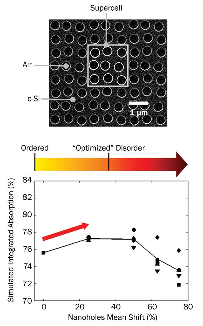
Introducing a controlled amount of position disorder within a periodically repeated supercell enables further increase of the integrated light absorptance of thin crystalline silicon (c-Si) active layers in the low absorption region (700 to 1000 nm). Courtesy of Lyon Institute of Nanotechnology.
For example, the research group of Thomas F. Krauss, now at the University of York in England, showed the large pitch size of supercells (larger than the longest wavelength to be harvested) can provide many diffraction orders, while the aperiodic elements are used to adjust the coupling efficiency of these orders3.
In this predictive approach, the sub-elements are irregularly arranged to trigger a phase shift between the diffraction orders, whereby the objective is to obtain destructive interferences for the lower orders, which do not couple to quasi-guided modes, and to reinforce coupling with higher orders that foster light trapping.
Other theoretical studies pointed out the benefits of introducing structural disorder in supercells, especially by slightly displacing each subelement (nanohole) in a random direction. For example, it was shown that breaking the symmetry of a 2D periodic PhC membrane leads to an increase in the density of modes and the number of new absorption peaks.
Moreover, the magnitude of the introduced perturbation can be tailored to reach a broadband absorption enhancement by adjusting the width of these new absorption peaks. In these designs, structural disorder is purposely exploited. This improves the coupling conditions over optimized periodic PhCs, which in turn necessitates careful control of the supercell size as well as the magnitude of the perturbation.
Notably, it was numerically demonstrated that clustering of nanoholes — giving rise to an effective light-scattering element with a larger dimension than isolated nanoholes — was detrimental because clustering introduced undesired spatial frequencies.
Supercells display a long-range order and also preserve a certain degree of correlation at a shorter scale, namely, a minimum distance between neighboring nanoholes. This “optimized disordered” design was successfully integrated in small-scale optical demonstrators by using electron-beam lithography followed by plasma etching so as to reach the high level of accuracy necessary.
To relax these design constraints and circumvent slow serial writing processes, long-range order should be avoided. By maintaining a short-range ordering within the nanoholes array, and if the characteristic dimensions describing the amorphous PhC are properly chosen, good light-coupling properties can be achieved in the relevant spectral range.
This strategy opens the route to rapid and upscalable nanopatterning techniques; a well-known example is self-stabilized colloidal lithography. Radwanul H. Siddique, Yidenekachew J. Donie, and colleagues from the Karlsruhe Institute of Technology in Germany have proposed a biomimetic approach inspired by the highly absorbent wings of the black butterfly (Pachliopta aristolochiae). These wings also rely on efficient light in-coupling (light channeling) and light-scattering disordered nanoholes4. It is believed that these nanometer-scale self-assemblies arise from the phase separation of lipid bilayer membranes of living cells.
An analogous but synthetic method, exploiting the lateral phase separation of binary polymer blends, was proposed to introduce disordered nanoholes into a resist layer while controlling their shape, diameter size distribution, and short-range ordering.
The transfer of this pattern into optical demonstrators based on thin a-Si:H layers proved this approach can lead to significantly improved light-harvesting properties (integrated absorptance increase of +93 percent relative to unpatterned a-Si:H layers measured at normal incidence) and is well adapted to the patterning of large-area PV active layers.
Nanopatterned solar cells
Despite remarkable absorptance gains reported in optical demonstrators, so far only a few nanopatterned active layers have resulted in functional thin-film solar cells with an improved power-conversion efficiency, with respect to unetched devices. The optical benefits of the first fabricated nanopatterned solar cells were counter-balanced by the degradation of their overall electrical performances. Because of the substantial surface area increase caused by nanopatterning, and the highly defective regions introduced close to the dry etched surfaces, the minority carrier lifetime decreased by up to two orders of magnitude as compared to the reference planar devices. Additionally, the first tests revealed that the steep nanohole sidewalls hinder the conformal deposition of the transparent conductive layer on the front side of the textured solar cells, leading to poor electrical contacts. Based on this experience, the PhC design was adapted from steep to inclined nanohole sidewalls that promote conformal deposition and further improve light in-coupling. Wet chemical etching was considered, strongly limiting the detrimental effects of surface recombination5.
Following that direction, an important milestone has been achieved by researchers from imec in Belgium and their collaborators, who have reported a doubled power-conversion efficiency upon integration of a disordered array of wet-etched nanoholes inside a 1.1-µm-thick monocrystalline silicon solar cell6.
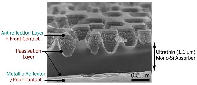
Ultrathin, monocrystalline silicon solar cells based on 1.1-µm-thick active layers achieve a power-conversion efficiency as high as 8.6 percent thanks to the broadband absorptance enhancement provided by the disordered nanohole array and the adapted etching and passivation processes. Courtesy of imec/LPICM/Chalmers Univ. of Tech.
Many past achievements helped to make this demonstration possible in a functional device. It took several generations of doctoral students, and simulation and experimental efforts by many scientists working in different research areas, to develop a light-harvesting design that could be integrated in a solar cell over large areas. Many photonic structures found in nature were instructional; structural disorder was found to be key to efficiently operating over a broad spectral and angular range. Considering the stability of these silicon-based solar cells, and their lightweight and flexible characteristics originating from the ultrathin layout, they could one day turn into a new generation of PV products. This could allow integration of solar cells in environments that are out of reach when using the commercially predominant wafer-based devices.
Meet the author
Guillaume Gomard, Ph.D., has worked on absorbing photonic crystals for photovoltaics at the Lyon Institute of Nanotechnology in Lyon, France. He is now leading a research group at the Karlsruhe Institute of Technology (KIT) to develop biomimetic, disordered, and printable materials for optoelectronic applications; email: [email protected].
References
1. P. Sheng et al. (1983). Wavelength-selective absorption enhancement in thin-film solar cells. Appl Phys Lett, Vol. 43, Issue 6, pp. 579-581.
2. Y. Park et al. (2009). Absorption enhancement using photonic crystals for silicon thin film solar cells. Opt Express, Vol. 17, Issue 16, pp. 14312-14321.
3. E.R. Martins et al. (2012). Engineering gratings for light trapping in photovoltaics: the supercell concept. Physical Review B, Vol. 86, Issue 4, p. 041404.
4. R.H. Siddique et al. (2017). Bioinspired phase-separated disordered nanostructures for thin photovoltaic absorbers. Sci Adv,
Vol. 3, Issue 10, p. e1700232.
5. C. Trompoukis et al. (2015). Photonic nanostructures for advanced light trapping in thin crystalline silicon solar cells. Physica Status Solidi (a), Vol. 212, Issue 1, pp. 140-155.
6. V. Depauw et al. (2017). Sunlight-thin nanophotonic monocrystalline silicon solar cells. Nano Futures, Vol. 1, Issue 2, p. 021001.