
Optical Interconnects Set to Achieve Bandwidth Benchmark
Silicon photonics interposer technology allows for low-power transceivers for 400-Gb/s optical interconnects.
By Johan Bauwelinck, Günther Roelkens, Philippe Absil, and Joris van Campenhout
Countless emails, text messages, pictures, and videos are posted on social media every day, along with unfathomable amounts of data that must be processed by the likes of Amazon and Google. All of this information must be stored and processed in data centers in the cloud. These data centers typically feature buildingwide optical fiber networks that comprise hundreds of thousands of optical links connected to server racks through a complex network of fiber optic cable.
Today, 100-Gb/s optical links — made up of four 25-Gb/s single channels or lanes — are sufficient to sustain the data traffic within a typical data center. These links transmit data over several hundreds of meters, up to 2 km. With social networking, cloud computing, and big data applications set to grow exponentially in the next few years, annual global data center IP (internet protocol) traffic is set to surpass 20 zettabytes (or 20 × 1021 bytes) by 2021, according to Cisco Global Cloud Index.
To meet this demand, data center operators will have to upgrade their network to 400-Gb/s links by 2019, and to 1.6 Tb/s by 2022. These next-generation 400-Gb/s optical links must cover 500-m, 1-km, and 2-km distances within the data center. Currently, the industry is considering implementing such links either with eight 50-Gb/s lanes or with four 100-Gb/s lanes to reduce the component count. Because of the vast number of optical links within a data center, they must be low-cost and consume as little power as possible.
Researchers from imec and imec/Ghent University in Belgium have investigated several implementations for optical links at ≥400 Gb/s using a silicon (Si) photonics platform. This platform integrates compact, high-speed modulators and photodetectors with electro-optical bandwidths beyond 50 GHz, and can be operated comfortably at 56-Gb/s NRZ (nonreturn-to-zero) single-lane data rates. By adopting higher-order modulation formats, single-channel data rates beyond 100 Gb/s can be realized. Two such complex modulation formats have been explored: the electrical duobinary (EDB) modulation format and the pulse-amplitude modulation format (PAM-4). Finally, the researchers address the electrical and optical packaging challenges in realizing fully integrated 50-GHz silicon photonics interposers, enabling tight integration of future multi-Tb/s optical modules with high-bandwidth logic and memory chips.
Prototyping platform
Single-mode fiber is the optical medium of choice for high-speed optical transceivers spanning 500 m, 1 km, or 2 km within a data center. Silicon photonics is ideally suited for integrating the essential building blocks of single-mode optical fiber links. With this scalable technology, compact and low-power transceivers can be implemented at low cost and high volume by leveraging existing CMOS fabrication infrastructure.
The imec researchers created a silicon photonics prototyping platform that uses 200-mm silicon-on-insulator (SOI) wafers as a starting substrate. The fabrication process uses a modified 130-nm CMOS flow augmented with 193-nm lithography for all of the waveguide patterning layers and germanium (Ge) for the photodetectors. An additional oxide/polysilicon stack is deposited to allow for more degrees of freedom in the design of the optical components. This stack is used for integrating the advanced silicon passive components, including fiber couplers, waveguides, and wavelength multiplexing filters. Subsequently, ion implantation, selective-area growth of germanium, and standard CMOS metallization modules are used to integrate active components, including electro-optic modulators, thermo-optic devices, and germanium photodetectors. Electronic circuits such as drivers and transimpedance amplifiers (TIA) can be fabricated on a separate wafer and assembled at the die level, with the silicon photonics circuits using flip-chip assembly methods. In these circuits, the driver converts a standard CMOS bit state into an electrical voltage or current that is compatible with the optical device, while the TIA translates the photocurrent back into a standard CMOS bit state.
56-Gb/s building blocks
Among the main building blocks of optical transceivers are optical modulators, which imprint data signals onto the optical carrier wavelength. Modulators can come in several forms, such as silicon ring modulators, silicon Mach-Zehnder modulators, and GeSi-based electroabsorption modulators — each having their own distinct properties and (dis)advantages. New variations of each of these modulators enable them to operate at 56-Gb/s NRZ, which is a simple two-level, one-bit modulation format, turning the light on or off depending on the bit state (1 or 0).
Carrier-based silicon Mach-Zehnder and ring modulators — originally developed for the C-band (1530- to 1565-nm wavelength) — have been optimized to operate in the O-band (1260 to 1360 nm). The O-band is the preferred band for applications requiring single-mode-fiber transmission distances beyond 1 km. Optimizations were based on design and process modifications. This has enabled the realization of a compact traveling-wave Mach-Zehnder modulator with 37-GHz bandwidth at −1 V bias, which is sufficient for 56-Gb/s NRZ operation.
Alternatively, ring modulators can be used at the transmitter side. By exploiting the optical resonance effect, ring modulators can offer reduced dynamic power consumption and a smaller footprint. However, they are more sensitive to temperature fluctuations and fabrication variability, and, as such, require a feedback-loop control circuit and integrated heater to stabilize the modulation performance. The research team developed O-band ring modulators with modulation bandwidths in the range of 35 to 45 GHz. With a 1-Vpp (volt peak-to-peak) driver, the 35-GHz modulator operates with ~3-dB extinction ratio and ~5-dB insertion loss. The integrated heater enables thermo-optic tuning and stabilization of the ring-operation wavelength across more than 100 °C.
Finally, a GeSi-based electroabsorption modulator was developed operating in the C-band. Such modulators in general offer a wider optical bandwidth than ring modulators, for instance. Additionally, when designed in a lateral PIN GeSi diode configuration, the same device can be optimized to work as a photodiode. This way, a single-chip silicon photonics transceiver — with both electroabsorption modulators and photodiodes — is achieved, operating with a bandwidth well beyond 50 GHz. A driver with a 2-Vpp swing driver realizes an extinction ratio of ~4 dB with similar optical insertion loss.
Toward 400-Gb/s optical links
A team from IDLab and the Photonics Research Group (both are imec research groups at Ghent University) used these modulators and photodiodes as building blocks to demonstrate advanced 100-Gb/s single-lane transmitters by applying the building blocks and combining them with advanced, dedicated high-speed electronics. The team explored and assessed three different modulation formats: NRZ, EDB, and PAM-4. With these 100-Gb/s transmitters, 400-Gb/s optical links can be built, either through the use of four parallel fibers (through which light of one specific wavelength is sent in parallel) or through wavelength multiplexing. With wavelength multiplexing, the signals are encoded onto four different carrier wavelengths that are transmitted through the same optical fiber.
The most obvious approach toward single-lane 112-Gb/s transmission is to double the speed of the original 56-Gb/s NRZ modulator. However, making the electronics fast enough to enable this high data rate is not straightforward. To do this, the researchers used an electrical transmitter (developed in-house) and receiver capable of generating and processing 100-Gb/s signals, together with a GeSi-based electroabsorption modulator. Transmitter and receiver chips were developed in a 0.13-µm SiGe BiCMOS technology (Bi-
CMOS integrates two semiconductor technologies — CMOS and bipolar junction transistors — into one device).
A key innovation was required to realize the first 100-Gb/s NRZ error-free transmission over 500 m in real time. On the transmitter side, an analog equalizer on-chip was applied to compensate for any bandwidth limitations in the subsequent electrical or optical components within the link. This compensation was achieved by predistorting the electrical signal that comes out of the transmitter. At 100-Gb/s NRZ, a bit error ratio (BER) down to 6E-9 was achieved for transmission over 500-m single-mode fibers.
However, at this high speed, chromatic distortion in the fiber channel becomes the limiting factor for transmission
>500 m. As a result, bandwidth is decreasing at larger distances, especially at 2 km. If a transceiver that covers all relevant distances in a data center — 500 m, 1 km, and 2 km, for instance — is required, a different approach is needed.
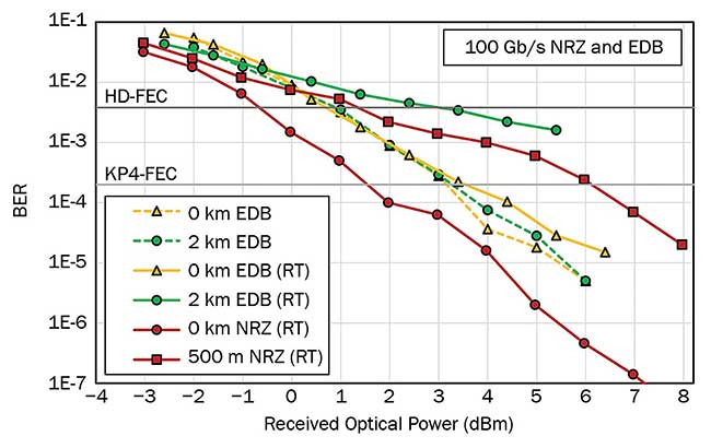
Figure 1. Bit error rate (BER) curves for 100-Gb/s NRZ (nonreturn-to-zero) and EDB (electrical duobinary)transmissions. RT: real-time measurement results; HD-FEC: hard-decision forward error correction; KP4-FEC: KP4 forward error correction. Courtesy of Imec.
In a second experiment, the researchers focused on EDB modulation because it is more resilient to this type of fiber distortion. The EDB modulation format is more complex than NRZ, but it provides improved performance for longer distances. In their experiment, the researchers used the bandwidth limitation of the channel, as observed in the first experiment, to shape the signal into a three-level signal. These three levels, denoted as −1, 0, and 1, are translated into three optical intensities, in contrast to optical duobinary modulation.
The EDB three-level signal also translates into a different eye diagram, which is a key metric for assessing the transmitter’s performance. In an eye diagram, an open eye typically corresponds to a minimal distortion of the signal. While NRZ transmission results in eye diagrams with one series of eyes, the EDB format results in two series of eyes (optimally, each with open eyes). Using this approach, the team was able to demonstrate the first real-time 100-Gb/s EDB transmission over more than 2 km of single-mode fiber (Figures 1 and 2).
Four-level modulation format
Only recently, the industry has adopted PAM-4 as the modulation format of choice for 100-Gb/s single-lane transmission over 500 m, 1 km, and 2 km distances. NRZ and EDB are two- and three-level modulation formats, respectively, but PAM-4 is a four-level modulation, with levels denoted as 00, 01, 10, and 11 (combining two bits in each level). NRZ ideally switches between “all of the light” (1) or “no light” (0), but PAM-4 levels correspond to “no light,” “a third of the light,” “two-thirds of the light,” or “all of the light.” With this four-level format, the data rate can be doubled while keeping the same bandwidth.
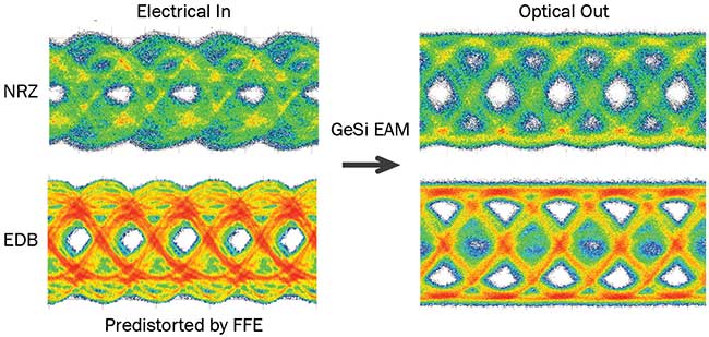
Figure 2. 100-Gb/s NRZ and EDB transmission: predistorted electrical signal applied to (left) and resulting optical signal after the GeSi electroabsorption modulator (EAM) (right). FFE: feed-forward equalization. Courtesy of Imec.
Generating and receiving PAM-4 at line rates of 112 Gb/s has proven very challenging. In general, using a multilevel modulation format leads to reduced eye openings. In addition, in a single-modulator implementation, the modulator needs to have a linear transfer function. Most types of modulators, however, are nonlinear devices. Attempts to solve this issue are mainly limited to the electrical domain and rely on power-hungry tools such as digital signal processing (DSP) and digital-to-analog converters (DACs). This way, they consume significantly more power than their NRZ counterparts at the same data rate.
The IDLab and the Photonics Research Group team realized a unique solution to enable low-power 112-Gb/s PAM-4 transmission. First, instead of going from bits to an analog signal in the electrical domain, they went from bits in the electrical domain to an analog signal in the optical domain. By using these digital-to-optical converters, the digital-to-analog conversion is postponed to the optical domain. And this significantly reduces the complexity and power consumption at the transmitter side.
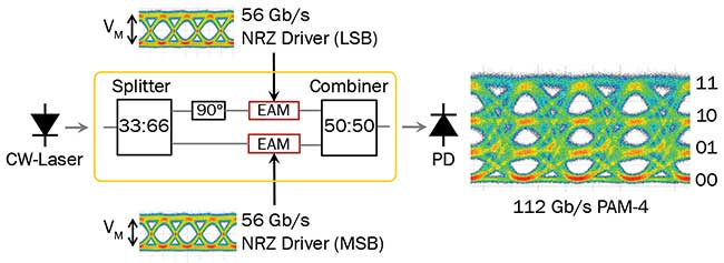
Figure 3. Proposed topology for the PAM-4 transmitter (left) and optical eye diagram (right). EAM: electroabsorption modulator; LSB: least significant bit; MSB: most significant bit; PD: photodetector; VM: modulation voltage. Courtesy of Imec.
Second, instead of using a single modulator, they proposed a novel transmitter topology based on the addition of two parallel 56-Gb/s NRZ electroabsorption modulators. By introducing a 33 percent/66 percent power split and a 90° phase difference between the two modulators, an equidistant PAM-4 eye can be obtained. Using this innovative solution, the linearity requirement is completely removed from the transmitter electronics and modulators. With this DAC-less and DSP-less transmitter, 112-Gb/s PAM-4 transmissions could be obtained over 2 km of single-mode fiber, with clear open eyes at 112 Gb/s (Figure 3).
Optical and electrical interfaces
Silicon photonics provides a highly integrated platform for incorporating silicon waveguides with active and passive components. Electronic circuits can be fabricated on a separate die and assembled with the silicon photonics circuits using flip-chip assembly methods. However, the optical module should connect to single-mode fibers, with low optical loss and acceptable packaging cost. The optical module also needs to interconnect to an application-specific integrated circuit (ASIC) or field-programmable gate array (FPGA) elsewhere in the package through high-density and high-speed electrical interconnects. Therefore, optical and electrical interfaces need to be integrated with the high-speed optical components discussed above, essentially realizing a silicon photonics interposer.
Key metrics for the optical interface are the optical coupling efficiency, spectral bandwidth, and sensitivity to polarization. For coupling to the single-mode fiber, imec has designed, fabricated, and tested optically broadband edge couplers, leveraging a hybrid platform consisting of a silicon photonic layer combined with a silicon nitride photonic layer. Innovations to the layer stack have enabled an optimized coupling efficiency of better than −2.5 dB for O-band operation, and better than −2 dB for operation in the C- and L-bands with less than 0.5-dB polarization sensitivity.
To enable dense high-speed electrical interconnections over short distances, 10-µm × 100-µm through-silicon vias (TSVs) have been integrated in the imec-developed silicon photonics platform on 300-mm SOI wafers. They connect the ASIC or FPGA to the CMOS driver and TIA circuits through the silicon photonics interposer. Performance measurements reveal high-speed TSVs, with electrical 3-dB bandwidth exceeding 50 GHz.
The silicon photonics interposer technology is suited for compact, low-power, and low-cost transceivers for ≥400-Gb/s optical interconnects. Using the silicon photonics prototyping platform, high-speed modulators and photodetectors have been developed, capable of operating at 56-Gb/s NRZ.
With these devices as key building blocks, single-channel data rates up to 112 Gb/s were demonstrated by using PAM-4, an advanced modulation format proposed by industry for 400-Gb/s optical links. Both NRZ and EDB provide an elegant and realistic alternative for
100-Gb/s single-lane optical channels. And, to enable a true 50-GHz silicon photonics interposer platform, broadband optical and electrical interfaces are proposed to enable efficient coupling with single-mode fiber and electrical chips, respectively.
Meet the authors
Johan Bauwelinck, Ph.D., is a professor at IDLab, an imec research group at Ghent University. His research focuses on high-speed, high-frequency integrated circuits; email: johan.bauwelinck@ugent.be.
Günther Roelkens, Ph.D., is a professor at the Photonics Research Group, an imec group at Ghent University, where he is leading the work on silicon photonics high-speed optical transceivers and III-V-on-silicon heterogeneous integration; email: gunther.roelkens@ugent.be.
Philippe Absil, Ph.D., is the director of the 3D and Optical I/O technologies department at imec and is responsible for the silicon photonics technology platform development; email: philippe.absil@imec.be.
Joris Van Campenhout, Ph.D., is director of the Optical I/O industry-affiliation R&D program at imec (Belgium). Prior to joining imec in 2010, he was a postdoctoral researcher at IBM’s Thomas J. Watson Research Center; email: joris.vancampenhout@imec.be.
/Buyers-Guide/Imec/c22187