Scientists have created a scale by which labs can determine the binding energy of excitons, and thus their bandgap structures, in perovskite quantum wells of any thickness.
The findings were based on a study of excitons trapped in quantum wells made of halide perovskite. The excitons used in the research were electrically neutral quasi-particles, which exist only when electrons and electron holes bind in an insulating or semiconducting solid, such as quantum wells. The quantum wells used in the study were based on perovskite compounds with a Ruddlesden-Popper phase (RPP) layered structure.
Scientists already knew that they could tune the resonance of excitons and free carriers within RPP perovskite layers by changing the perovskite layer thickness. However, they did not know how to measure the change in exciton mass.
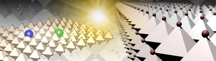
An artist’s depiction of interacting electronic charges forming a strongly bound exciton trapped in an atomic-thick layer of hybrid perovskite. The colored balls represent an electron and a hole (the pair makes up the exciton). Pyramids (octahedra) sketch the crystal structure of the 2D perovskite. Courtesy of Jean-Christophe Blancon/Los Alamos National Laboratory.
“Varying the thickness of these semiconductors gave us a fundamental understanding of the . . . physics between monolayer 2D materials and 3D materials,” said Los Alamos scientist Jean-Christophe Blancon.
Researchers at Los Alamos National Laboratory tested the quantum wells under a 60-tesla magnetic field to directly probe the effective mass of the excitons. The well samples were then brought to Rice University, where a spectroscope was used to expose the samples to ultralow temperatures, high magnetic fields, and polarized light simultaneously.
Understanding the nature of excitons and generating a general scaling law for exciton binding energy is the first step in optoelectronic device design.
Los Alamos researchers used spectroscopy to probe the optical transitions within the RPP perovskite compounds. The exciton binding energies were derived from this step.
Researchers matched results of the probe to a computational model and determined that the effective mass of the excitons in perovskite quantum wells up to five layers was about two times larger than in their 3D bulk counterpart.
As the wells approached five layers (3.1 nm), the binding energy between electrons and holes was significantly reduced but still larger than 100 meV, making the energy robust enough to exploit at room temperature, said Blancon.
By combining experimental and computer model data, researchers were able to create a scale that predicts exciton binding energy in 2D or 3D perovskites of any thickness. Researchers further found that perovskite quantum wells above 20 atoms thick (about 12 nm) transitioned from quantum exciton to classical free-carrier rules normally seen in 3D perovskites at room temperature.
The researchers noted that though the experiments were carried out at ultracold temperatures, what they observed should also apply to room temperature.
“This work represents a fundamental and nonintuitive result where we determine a universal scaling behavior for exciton binding energies in Ruddlesden-Popper 2D hybrid perovskites,” Los Alamos scientist Aditya Mohite said.
“This is a fundamental measurement that has remained elusive for several decades, but its knowledge is critical before the design of any optoelectronic devices based on this class of materials, and may have implication[s] in the future for design of, for example, zero-threshold laser diodes and multifunctional heteromaterial for optoelectronics.”
The research was published in Nature Communications (doi:10.1038/s41467-018-04659-x).