 LED Constant Voltage Drivers
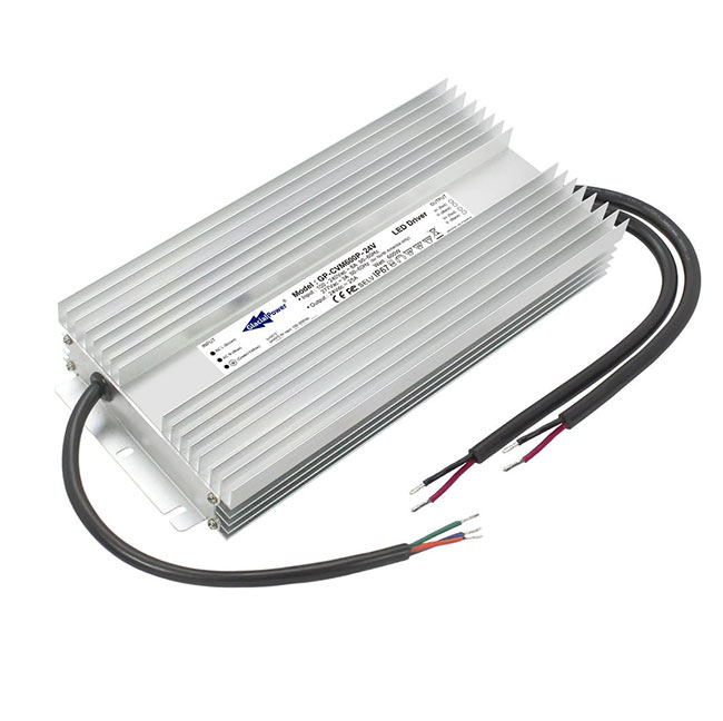
The GP-CVM600P series of 600-W LED constant voltage drivers from GlacialPower include nondimming, 3-in-1, and DALI-2 dimming versions.
The direct-current output voltages include 12, 24, 36, 48,...
Photonics Spectra July 2023 Issue