
Self-Assembly Eases Fabrication of Photonic Crystals
Richard Gaughan
Devices constructed of photonic crystals promise to enable the precise, localized control of optical propagation. The fabrication of such crystals usually involves a complex and expensive multistep process. However, researchers at the University of Toronto recently developed a self-assembly crystallization process that points to the cost-effective production of functional photonic bandgap circuit components.
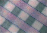
An optical micrograph reveals a "Lincoln log" architecture based on opal microchannels developed by researchers at the University of Toronto. Bragg diffraction causes the red color. Courtesy of Geoffrey A. Ozin.
Adopting techniques that are analogous to self-assembly in natural opals, Geoffrey A. Ozin and his colleagues, Hernan Miguez and San Ming Wang at the university's Materials Chemistry Research Group, condense silica microspheres from colloidal suspensions into crystalline opal structures.
Naturally occurring opal forms when silica spheres precipitate from solutions or colloidal suspensions into seams or crevices in surrounding rock. Most opal is amorphous, but the silica spheres in precious opal organize into a face-centered-cubic structure well-suited for photonic bandgap crystals because of the index variation between the silica spheres and the interstitial material.
To fabricate the photonic crystals, the researchers begin by creating a variety of microchannel architectures in which the crystals will form using photolithography and other micromachining techniques. For example, they prepared a silicon substrate with an arrangement of 25-µm-wide vertical channels and immersed it in a colloidal suspension of silica microspheres in alcohol. The microspheres self-assembled exclusively within the channels in a face-centered-cubic structure.
To demonstrate the potential for tuning the photonic bandgap of the synthetic opal crystals, the researchers developed a modulated-thickness mold, in which the channels accommodated either 18 or 21 closely packed layers of 315-nm-diameter microspheres. Modeling predicted a 10 to 12 percent variation in the width of the reflectance peaks across the layers. Employing a scanning optical microscopy/spectroscopy method developed for probing the properties of colloidal photonic crystals, they discovered that the reflectance of the 10 x 10-µm sections of each crystal thickness matched the theoretical prediction.
By varying the form of the mold in which the microspheres assemble, the team can create crystals of different thicknesses or orientations. And the technique is especially effective because the crystals that result already are in a physical format that is appropriate for integration with various photonic devices, such as those for telecommunications applications.
"This is a simple, fast, reproduc-ible and cost-effective method," Ozin said, "which fuses concepts and methods in microfabrication and self-assembly."
Published: September 2002