Martin Waeny, Awaiba CH SA
Wafer-level packaging, CMOS circuits and MOEMS technologies help realize sub-1-mm camera modules.
Imaging and small-sized digital camera modules have become ubiquitous. Only a few years ago, a digital camera recorder was still a considerable investment, and its size and weight made users consider whether to drag it along or not. Today, the presence of digital cameras everywhere seems self-evident. Smartphones usually implement more than one camera, and game consoles are gearing up to combine video, digital stills and 3-D interaction with the total gaming experience, resulting in four or more cameras per device.
The expansion of cameras has only been possible by their miniaturization, both in size and in cost. As with many innovations in the electronics business, the engine behind driving down size and cost, as well as increasing performance, comes from the semiconductor manufacturing industry’s Moore’s law, which predicts that the size of transistors will halve – and, consequently, performance of integrated semiconductor devices will double – every 1.5 years. The outcome of this race to ever-smaller and better-performing digital processor and memory chips can be applied to digital imaging, making it now possible to realize image sensors with pixels as small as 1 μm. This is driven mainly by the consumer electronics industry, where 1.1-μm pixel size is in mass production and some companies are already working on 0.9-μm pixels.
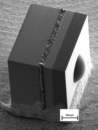
This scanning electron microscope image shows the NanEye’s 1-mm camera module with wafer-level lens. Courtesy of Awaiba.
The standard mobile-device camera module, however, still measures some 4 to 5 mm in each dimension, primarily because of the system-cost optimization realized by combining many image preprocessing functions on the image sensor itself and by using plastic injected components for lens holders and overall housing.
To slim modules down, an effective approach is to remove everything not imperatively needed for the bare imaging task, and to combine the sensor technology with optics and assembly that will not add to the overall module size. One instrument that resulted from this approach was a digital camera module that Awaiba presented in 2008 with a side length of 500 × 500 μm and a build height of only 0.9 mm, including a wide-angle lens.
It was used in the NanEye off-the-shelf product family, which offers a 1 × 1-mm footprint, a 1.4-mm build height and several integrated optics variations to provide images at 62K pixels in full-digital format.
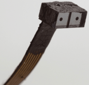
The NanEye Stereo module is designed to enable 3-D vision. Courtesy of Awaiba.
Applications
The first applications of this technology appeared in established endoscopic procedures with reusable flexible endoscopes, where the miniaturized camera modules replaced the fiber optic image bundles, thereby increasing the resolution and image quality. The camera modules also enabled more flexible scopes that can take narrower turns or flex into places and viewing angles not previously reachable. The first realized applications of reusable scopes with such miniaturized digital camera modules were urethroscopes and laryngoscopes. Compared with fiber image bundles, the chip on the tip-camera modules can provide resolution about two to three times higher.
Single-use devices are possible with the technology due to the possible lower cost at high volume, compared with that of fiber bundles. The big drivers behind single-use endoscopes are patient safety (especially flexible endoscopes, which are extremely difficult to clean reliably) and patient cross infection, an ever-increasing concern. Further, the cost of sterilization and equipment management incurred with reusable equipment can be avoided by using off-the-shelf single-use devices.
The NanEye 2-D standard camera module provides 62K pixels, which is an advantage over 15K to 20K fiber optic bundles that cause strong honeycomb image artifacts in addition to providing limited resolution. Courtesy of Awaiba.
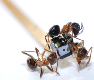
The availability of moderate-cost disposable camera modules further enables visualization for devices that operated blindly before, from guide wires to electrosurgical probes. The Nathaniel Group of Vermont has integrated mini camera modules in a visualization module with only a 2-mm outer diameter, together with two illumination fibers for a disposable single-use probe, for a manufacturer of an endoscopic device targeted at screening and on-site biopsy analysis for cancer. Other customers have integrated the modules into disposable electrosurgical probes used in cardiac surgery.
A further driver of disposable endoscopy devices with miniature digital camera modules is the move of endoscopic procedures out of the operation theater and into the doctor’s office. A 1-mm camera module can be integrated into a surgical needle and may be applied by puncture rather than by incision, which will greatly reduce the complexity and cost of the procedure.
Technology
Minimizing the footprint of a digital camera module meant first rethinking the digital image sensor itself. Current standard digital image sensors for mobile phones, webcams or other applications embed a number of functionalities and follow architectures suitable for scaling up to resolution of several megapixels. This results in only part of the chip surface being used for the actual pixel matrix, while a considerable peripheral area is used for column-parallel analog digital converters, low-power charge pumps, automatic exposure control and, possibly, color reconstruction algorithms and mobile processor interfaces. Such features require not only chip area in the periphery of the matrix, but often also external components for voltage stabilization in the vicinity of the image sensor.
For minimal module size, we stripped the chip of any features that were not absolutely mandatory and redesigned the others to achieve a chip periphery below 90 μm on each side of the matrix, even with a chip size of less than 1 mm. On a chip with 700-μm side length, this leaves less than 0.2 mm2 for all peripheral electronics. (In a digital mobile phone imager, the digital interface controller could take up this area all by itself.) Further, the chip architecture was optimized to avoid the need for passive components such as decoupling capacitors close to the chip. This arrangement allowed the camera heads to work with up to 3 m in cable length and reliably transmit the digital output signals without coaxial shielding cables or the loss of image quality due to electromagnetic interference.
Of course, the size-optimized image sensor by itself is not enough to build the smallest camera modules. To permit chip packaging on such a small footprint, the electrical connection to the imager is made by chip-scale packaging technology, which provides the electrical contact from the electronics to the outer world by “drilling” tiny via holes through the silicon and connecting solder balls on the back side to the active electronics on the front side. This technology, known as TSV (for through-silicon via), allows the overall device and package size to be kept exactly to the outline of the image sensor circuit and does not require extra area for bond wires or connections over the device sides.
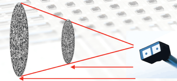
This schematic shows the principle of distance measurement with the NanEye Stereo module and its pseudorandom pattern projector. Courtesy of Awaiba.
Finally, as any hobby photographer knows, the greatest camera body is worthless without an adequate lens. However, when the camera shrinks to the 1-mm scale and smaller, optics and especially their precise placement become challenges in and of themselves. To mitigate this, we used technologies from optical and mechanical microsystems manufacturing (such as the processes used to make acceleration and tilt sensors in a tablet) to etch lenses out of quartz glass wafers and to assemble the full stack on the CMOS image sensor wafers. This approach is a unique technology developed by Awaiba with the Fraunhofer Research Institute. Apart from miniaturization, it also provides a great economy of scale: When slicing up pizza-sized wafer stacks into 1-mm or smaller camera modules, several thousand cameras result from a single stack, allowing for incredibly low cost at high volumes.
Outlook
For the future, plain visualization tasks will see the normal scaling of resolution, evolving two paths. One path will provide even higher resolution with the same module size – but coming from an industry following Moore’s law, this is a no-brainer. The other path will see ever-smaller modules with approximately the same resolution. We have already shown that 500 × 500 μm is possible, and our studies show that even 300 × 300 μm would be possible, provided that a particular application finances the up-front development cost.
Apart from 2-D visualization, the mini optical modules can introduce a third dimension to visualization by placing two cameras adjacent to each other. Technical University of Munich embedded a stereo version of the NanEye camera modules in a surgical robot to teach it to tie knots with the surgical string and needle used in microinvasive surgical procedures.

This image was taken by the NanEye 2-D camera module in human trial. Courtesy of The Nathaniel Group.
For this, we developed a pseudorandom pattern projector and combined two mini camera modules; they were perfectly aligned in parallel due to the full-wafer manufacturing approach. The pseudorandom pattern projector mapped the contrast picture from the two cameras and created a 3-D point cloud that allowed the robot to find the 3-D position of needle and string; it then could perform the knot tying autonomously. Try to do this one-eyed and one-handed to get an impression of the challenge; then imagine having to teach this to a machine working inside your stomach.
A less complicated use of the 3-D capability of these camera modules is simply the repeatable measurement of dimensions – for example, when assessing whether a lesion is growing or stable, a frequent task in women’s health care. When doing this by endoscopy, knowing the exact distance between the scope and the tissue is mandatory for performing a repeatable measurement.
Meet the author
Martin Waeny is the CEO of Awaiba CH SA in Yverdon-les-Bains, Switzerland; email: [email protected].