MOSCOW, Russia, Jan. 21, 2016 — A team from the Moscow Institute of Physics and Technology (MIPT) has found that a cooling system employing high-performance thermal interfaces can be used to mitigate the heat generated in optoelectronic chips.
Self-heating of active plasmonics, which limits achievable optical gain, has been a barrier to the development of optoelectronic microprocessors for high-speed data transfer. As the semiconductor industry looks to replace electrons with photons to increase data-transfer capabilities, they must also address the challenge of scaling down photonic components.
The speed of multicore and manycore microprocessors, which are already used in high-performance computer systems, depends on the takes for data to be transferred between the cores. The electrical copper interconnects used in microprocessors today are fundamentally limited in bandwidth, and they cannot be used to maintain the continuing growth of the processor performance.
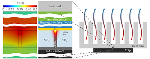
Temperature distribution in an active plasmonic waveguide on an optoelectronic chip with a cooling system. Courtesy of the MIPT.
Replacing electrons with photons could enable large amounts of data to be transferred between processor cores almost instantly, which in turn means that the processor performance will be nearly proportional to the number of cores. However, due to diffraction, photonic components are not as easy to scale down as electronic components. Their dimensions cannot be smaller than the size approximately equal to the light wavelength (about 1000 nm, or 1 μ), but transistors will soon be as small as 10 nm.
This fundamental problem can be solved by switching from bulk waves to surface waves, which are known as surface plasmon polaritons (SPPs), enabling the confinement light on the nanoscale.
The main challenge to the transition is that SPPs are absorbed by metal, a key material in plasmonics. The effect is similar to resistance in electronics, where the energy of electrons is lost and converted into heat when current passes through a resistor. The SPP loss can be compensated by pumping additional energy into the SPPs. However, this pumping will produce additional heat; this will cause an increase in temperature not only in the plasmonic components, but also in the processor as a whole.
The higher absorption in the metal, the greater the loss, and the stronger pumping will be required. This raises the temperature, which again causes a loss increase and makes it more difficult to create the optical gain that is required to compensate for the loss; subsequently, more powerful pumping is required. A cycle is formed in which the temperature can rise to such an extent that a processor chip simply burns out.
The heating power per surface unit of the active plasmonic waveguide with loss compensation exceeds 10 kW/cm2, said MIPT researchers. This is twice as high as the intensity of solar radiation at the surface of the Sun.
The MIPT team, led by Dmitry Fedyanin and Andrey Vyshnevyy, has now demonstrated the use of high-performance thermal interfaces — layers of thermally conductive materials placed between the chip and the cooling system — to efficiently remove heat from the system. The researchers used industry-standard heat sinks. Fedyanin and Vyshnevyy explain their work in the video below.
Based on the results of numerical simulations, the researchers concluded that if an optoelectronic chip with active plasmonic waveguides is placed in air, its temperature will increase by several hundred degrees Celsius, which would cause the device to malfunction.
However, multilayered thermal interfaces of nano- and micrometer thickness, combined with simple cooling systems, reduced the temperature of the chip from several hundred degrees to approximately 10 °C with respect to the ambient temperature.
The researchers said the work opens the prospects for the implementation of high-performance optoelectronic microprocessors in a wide range of applications, ranging from supercomputers to compact electronic devices.
The research was published in ACS Photonics (doi: 10.1021/acsphotonics.5b00449).