Optoelectronics applications may soon be built using monolayered 2D heterostructures made from materials using mismatched lattices.
In a study led by the U.S. Department of Energy’s Oak Ridge National Laboratory (ORNL), scientists synthesized a stack of atomically thin monolayers of two lattice-mismatched semiconductors. Where the two layers met, they formed an atomically sharp heterostructure, which generated a photovoltaic response by separating electron-hole pairs that were generated by light.
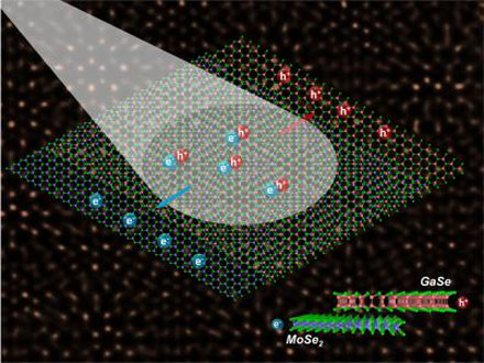
Light drives the migration of charge carriers (electrons and holes) at the juncture between semiconductors with mismatched crystal lattices. These heterostructures hold promise for advancing optoelectronics and exploring new physics. The schematic's background is a scanning transmission electron microscope image showing the bilayer in atomic-scale resolution. Courtesy of Oak Ridge National Laboratory, U.S. Department of Energy. Image by Xufan Li and Chris Rouleau.
“Because the two layers had such a large lattice mismatch between them, we did not expect them to grow on each other in an orderly way — but they did,” said ORNL researcher Xufan Li. “It’s a new, potential building block for energy-efficient optoelectronics.”
The creation of an atomically thin solar cell may facilitate synthesis of mismatched layers to enable new families of functional 2D materials. The research broadens the number of materials that can be combined, thus creating potential for a wider range of atomically thin electronic devices.
"These new 2D mismatched layered heterostructures open the door to novel building blocks for optoelectronic applications," said researcher Kai Xiao of ORNL. "They will allow us to study new physics properties which cannot be discovered with other 2D heterostructures with matched lattices."
For the study, Li first grew a monolayer of molybdenum diselenide, and then grew a layer of gallium selenide on top. This technique, called van der Waals epitaxy, is named for the weak attractive forces that hold dissimilar layers together. "With van der Waals epitaxy, despite big lattice mismatches, you can still grow another layer on the first," Li said. Using scanning transmission electron microscopy, the team characterized the atomic structure of the materials and revealed the formation of Moiré patterns.
Researchers in ORNL’s Functional Hybrid Nanomaterials group conducted the study with partners at Vanderbilt University, the University of Utah and Beijing Computational Science Research Center. The scientists plan to conduct future studies to explore how material composition influences properties beyond the photovoltaic response, in order to incorporate 2D materials into devices.
The atomically thin layers that comprise 2D heterostructure also have potential uses in clean energy and optically active electronics. To learn more about the study of 2D semiconductors and their potential use in integrated nanophotonics, visit 2D Semiconductors Preserve Excitons, Explored for Integrated Nanophotonics.
The research was published in Science Advances (doi: 10.1126/sciadv.1501882)