Scientists are developing an entirely new generation of ultrathin materials such as graphene and germanene, whose photonic properties promise a new frontier of components and devices.
Graphene is a wonder material: a sheet of pure, stable carbon in a honeycomb-shaped lattice, one atom thick. It’s lightweight, 100 times stronger than steel and a highly efficient conductor of heat and electricity when doped. These properties lend it enormous potential as an alternative to silicon-based technologies like chips, LEDs and solar photovoltaics.
Research in graphene has rocketed since 2004, when Dr. Andre Geim and Dr. Kostya Novoselov at the University of Manchester in England first produced
it reliably in the lab. Their work precipitated a deluge of new research into the material’s properties and potential applications, garnering them the Nobel Prize in physics in 2010.
As silicon-based technology reaches the limits of miniaturization, graphene appears to be a promising replacement. In some applications, it may be a game changer.
High-quality graphene has proved relatively easy to produce and isolate. Graphene’s two-dimensional nature makes it transparent, yet it interacts strongly with light at wavelengths ranging from ultraviolet to microwave (doi: 10.1109/jproc.2013.2250892). Scientists recently discovered that stacking two sheets of graphene creates a bandgap similar to that of a semiconductor, which is tunable with an electric field so that it acts as a photovoltaic cell or LED.
Researchers at the University of Maryland in College Park and Monash University in Victoria, Australia, measured this bandgap using infrared light and found that the conductance of bilayer graphene was greater than that of the commercial silicon photodetector used to measure the power of the IR beam. Dr. Michael Fuhrer, professor of physics at both the University of Maryland and Monash, and colleagues also discovered that the conductivity of bilayer graphene is strongly correlated with electron temperature, enabling a hot-electron bolometer that can be used as a highly sensitive detector in radio astronomy.
Fuhrer and colleagues took the bilayer graphene one step further to create a photothermoelectric detector that works in the far-IR or terahertz region at room temperature (Figure 1). Terahertz wavelengths are already used in airport body scanners and imaging, as they can “see” through clothing, paper, cardboard and wood without the ionizing effects of x-rays. But terahertz radiation is notoriously difficult to detect at room temperature.
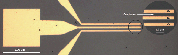
A broadband ultrafast graphene detector with chromium and gold leads can detect terahertz frequencies at room temperature. Photo courtesy of Thomas Murphy/University of Maryland.
To sense low-energy photons, the detectors must be kept at very low temperatures, which makes them bulky, slow and very expensive. The graphene terahertz detector developed by Fuhrer and colleagues is as sensitive as state-of-the-art commercial room-temperature detectors, exceeding 10 V W-1, but it would be much more inexpensive and up to a million times faster (doi: 10.1038/nnano.2014.182). Such terahertz detectors could be useful in all kinds of imaging applications, including fast Fourier-transform IR spectroscopy, inexpensive night-vision goggles and IR cameras, and mobile communications.
Fuhrer sees potential for such sensitive terahertz detectors in gathering IR light emitted by the Earth and turning it into electricity. “We could put detector dishes in the sky, facing the Earth, gathering radiant energy on clear nights,” Fuhrer said. “The energy per photon is small, so traditional photovoltaics don’t work very well. You might not need an area much larger than you would for traditional photovoltaics.”
Graphene nanoribbons
Materials scientists are only beginning to discover all the ways the new developments in nanomaterials can be applied. In 2013, a team of materials engineers led by Dr. James Tour, professor of chemistry, computer science, materials science and nanoengineering at Rice University in Houston, created a graphene-based deicing coating for sensitive military radar domes to replace the conventional metal-oxide structures that were bulky and energy wasting. Tour’s laboratory team designed a hexadecylated graphene nanoribbon film by splitting multiwalled carbon nanotubes (CNTs) into flat ribbons and spray-coating them onto a surface, followed by a polyurethane film (Figure 2) (doi: 10.1021/am503478w). Passing a voltage across the coating melts ice at constant temperatures down to −20 °C. The film transmits up to 2 × 10⁵ W/m2 of radio-frequency power at 99 percent transmittance.
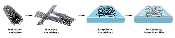
High-density graphene nanoribbon film is conductive, so it can keep ice and condensation away, but it is highly transparent to optical and radio wavelengths of light. Photo courtesy of J.M. Tour/Rice University.
The new thin film is easily dispersed by spraying, spin-coating or painting it onto almost any surface, creating a film of consistent thickness between 50 and 200 nm. As such, Tour’s group recently confirmed that the graphene nanoribbon coating also would work on glass, where it performs much like tinted glass, except that it can prevent vehicle windows or buildings from icing up. Because the material is transparent to radio frequencies, buildings or autos built with the material would better enable cellphone and Wi-Fi transmission. The coating technology can easily be scaled to conformal, large-scale film production to make it inexpensive.
Scientists from Tohoku University in Japan recently found another interesting and practical application for CNTs – a lightbulb that improves even upon LEDs. Associate professor of environmental studies Norihiro Shimoi and colleagues at Tohoku University in Sendai, Japan, and DOWA Holdings of Chiyoda-ku, Japan, fabricated an energy-efficient planar (flat) light source comprising single-walled CNT field emitters on a phosphor screen (Figure 3). The light source uses a hundred times less power than an LED – or around 0.1 W/h of operation – and can be produced easily at low cost (doi: 10.1063/1.4895913).
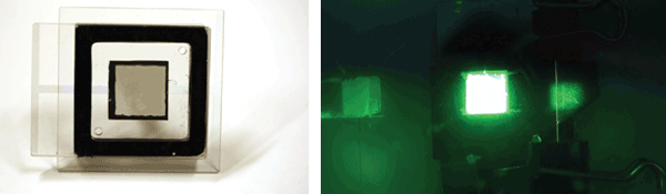
(a) Stand-alone flat plane-emission diode panels made from single-walled carbon nanotubes glow brightly and homogeneously green through a neutral-density filter; (b) a promising eco-conscious alternative to LEDs and conventional lightbulbs. Photo courtesy of Norihiro Shimoi/Tohoku University.
The Japanese group assembled the device from a mixture of crystalline single-walled CNTs in an organic solvent and a surfactant. They painted the mixture onto the surface of a cathode and applied a strong electric field to produce field emission, which caused the phosphor screen to glow. Unlike the diode structure of LEDs, the needle-shaped CNTs in the devices act as cathodes, with the phosphor screen acting as the anode. The simple panel can obtain a brightness efficiency of 60 lm/W, compared with hundreds of lumens per watt for LEDs and around 40 lm/W for organic LEDs. The device could work in consumer lighting or as a new type of ultraviolet emission source.
“We are now designing a new flat panel with very low power consumption using the prototype device,” Shimoi said. “We hope our device will someday contribute to reducing carbon dioxide emissions as part of a new approach to lighting in a comfortable lifestyle.”
Meet graphene’s cousins
As the synthesis of graphene has become more well understood, other new building-block nanomaterials with photonic properties are popping up. In Europe this October, a research team reported the first synthesizing of two-dimensional germanene, a “cousin” of graphene. Germanene was first proposed in 2009 but remained elusive until researchers in Spain, Germany and France managed to grow a one-atom-thick layer of germanium on a gold surface using molecular beam epitaxy (doi: 10.1088/1367-2630/16/9/095002). Research team leader Dr. Guy Le Lay at Aix-Marseille University in France and colleagues confirmed the telltale honeycomb geometry in parallel with an independent group in China (Figure 4).
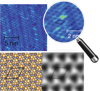
(Top) Germanene’s two-dimensional honeycomb structure appears in a 16.2 nm2 scanning-tunneling microscopy image of the √7 × √7 superstructure, and magnified atomic structure (in blue). (Lower left) Atomic structure and (lower right) simulated scanning-tunneling microscopy images of different models of germanene on a √7 × √7 Au(111) surface. Photo courtesy of New Journal of Physics/IOP Publishing.
Like graphene, germanene could be useful as a robust topological insulator at room temperature, making it a good candidate material for use in quantum computing. The first synthesis of this non-natural material was considerably demanding and marks only the beginning of a long quest to pursue ways to manufacture it more easily and to further characterize its properties, according to Le Lay.
Other candidate nanomaterials include titanium sulfide (stanene), which has potential in smaller, faster and more energy-efficient computers, and transition metal dichalconides such as molybdenum disulfide (MoS2), molybdenum diselenium (MoSe2) and tungsten disulfide (WS2). A group led by Dr. Kevin Huang, senior research fellow at the University of Southampton’s Optoelectronics Research Center in England, successfully fabricated ultrathin sheets of MoS2 on a variety of substrates measuring over 1000 mm2 using a chemical vapor deposition process (doi: 10.1039/C4NR04228J). With similar properties to graphene, MoS2 is a two-dimensional transition metal dichalconide that, unlike graphene, provides a tunable bandgap in a single layer. This makes it useful in transistors, photodetectors and biosensing devices.
With most of the new types of nanomaterials, continuing exploration will enable a new generation of devices that reduce cost, increase efficiency and address ease of manufacturing in numerous novel nanoelectronics and optoelectronics applications.