
$10B Earmarked for Extreme-UV Lithography Center
A high-numerical aperture extreme-ultraviolet (NA EUV) lithography center is set to be built at the NanoTech Complex semiconductor research facility in Albany, N.Y.
The state of New York partnered with IBM, Micron, Applied Materials, and Tokyo Electron, among others, to invest in expanding NY CREATES’ Albany NanoTech Complex where IBM is one of the key members.
The $10 billion investment will lead to the first and only publicly owned high NA EUV center in North America.
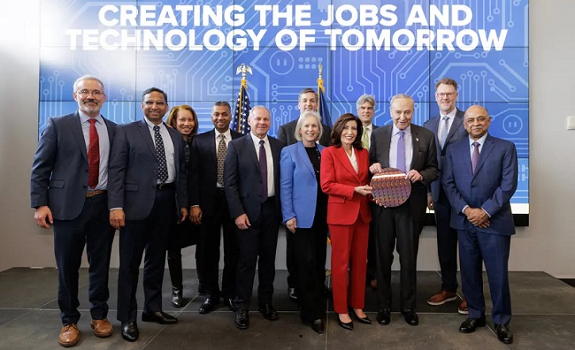
From right: IBM CEO Arvind Krishna, U.S. Sen. Chuck Schumer, N.Y. Gov. Kathy Hochul, and leaders from the semiconductor industry at the announcement of the high NA EUV center. Courtesy of Mike Groll/Office of Gov. Kathy Hochul.
The initiative, which state and industry officials announced Monday, calls for NY CREATES to acquire and install a high NA EUV lithography tool designed and manufactured by ASML. The instrument performs a technique in which lasers beyond the UV spectrum etch pathways in circuitry at a miniature scale. The process, which could first etch channels for 7 nm and then 5 nm chip processes a decade ago, now has the potential to develop and produce chips at nodes smaller than 2 nm — a barrier overcome by IBM in 2021.
EUV machines currently on the market and used by industry are unable to produce the resolution needed for sub-2-nm nodes to be patterned into chips in a way that would be conducive to mass production. Though the current generation of machinery can deliver necessary levels of precision, three or four exposures from the EUV light are required, rather than a single exposure, according to IBM. The addition of a high NA allows for larger optics that support higher-resolution patterns to be printed on wafers.
Although researchers will need to account for a shallower depth of focus, caused by the increased aperture, IBM and its partners believe that the technique can lead to the adoption of more efficient chips in the near future.
Construction of the new 50,000-sq-ft facility will begin in 2024.
/Buyers_Guide/ASML/c25112