An emerging class of ultrafast lasers has streamlined packaging and controls to allow end users in multiple end markets to leave their breadboards behind and get to work.
DARRYL MCCOY AND MARCO ARRIGONI, COHERENT INC.
To say that femtosecond laser technology has undergone a transformation in recent years is an understatement that not only minimizes the huge strides made in technical terms, but especially so the improvements in accessibility. Complex tabletops crowded with user-built assemblies and myriad discrete optics requiring daily attention have given way to single-box systems tailored to meet the fast-changing world of femtosecond applications. Early examples of this transition are tunable lasers for multiphoton microscopy, rapidly followed by powerful industrial one-box lasers developed to support micromachining applications ranging from stent cutting to OLED processing.
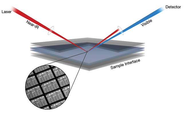
Femtosecond laser pulses can generate a small amount of second-harmonic light from the interface between two materials, or from any material that is noncentrosymmetric. The second-harmonic light signal generated can nondestructively detect and image features on and below the surface of semiconductor wafers, such as structural defects, film quality, and even trace metal contamination. Courtesy of FemtoMetrix.
Today, the latest examples of this evolutionary trend include a family of shoebox-size sealed lasers in the <5-W power range, with fixed wavelengths at key operating points, including 780, 920, and 1064 nm. These user-friendly lasers further provide application-relevant parameters, such as short pulse widths and high beam quality, pre-compensation to optimize the final pulse width, and fast modulation and control of the output power.
This new generation of ultrafast lasers was specifically optimized to support user demands in end markets such as additive manufacturing, medical science, semiconductor metrology, and applied research.
Nanoscale fabrication
Lasers find use in a number of additive manufacturing (AM) processes, including laser sintering of metals and stereolithography of polymers. These processes each provide a way to create complex and unique structures without the need for masks or molds. Additive manufacturing is particularly valuable for small-scale production applications, such as rapid prototyping of parts or for individualized medical implants.
An emerging AM method is a type of stereolithography called two-photon polymerization, which is rapidly gaining interest for several reasons. First, it is capable of higher spatial resolution than any other AM method. Second, it is a three-dimensional freeform process, so it is not constrained by the processing limitations of laser sintering or one-photon stereolithography, where the part must be created layer by layer from the bottom up or the top down.
The advent of compact, hands-free femtosecond lasers is making techniques such as two-photon polymerization more economically viable for a number of industries and applications.
How does the laser technology achieve this? In stereolithography, a laser beam is focused into a bath of photosensitive resin. When light of the right wavelength (usually in the ultraviolet) hits this resin, it breaks the polymer’s bonds and the material becomes reactive, forming a solid polymer from the liquid monomer chemical.
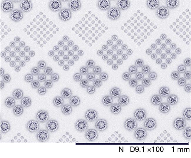
Two-photon polymerization, a three-dimensional freeform additive manufacturing technique with comparatively high spatial resolutions, is capable of producing extremely small parts and features. New femtosecond lasers are making two-photon polymerization techniques more economically viable. Courtesy of Wildman Lab/University of Nottingham.
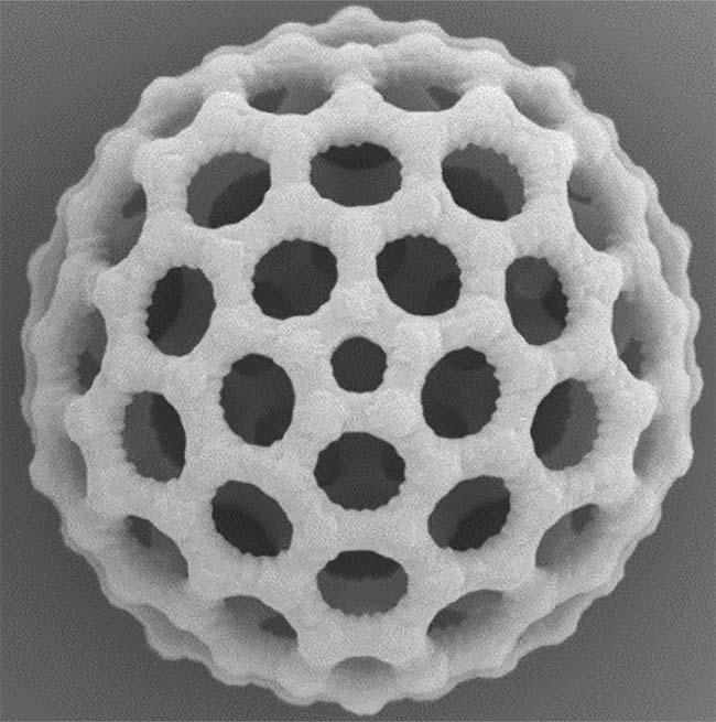
This process allows almost any shape to be created directly from a CAD file, and the raw materials are not expensive. In the two-photon approach, an ultrafast laser is tailored to double the normal wavelengths that the resin normally absorb. By using high numerical aperture (NA) optics, the beam is focused to a tiny waist. At this waist, and only at this waist, the peak power of the ultrafast pulses is high enough to drive two-photon absorption.
This approach provides unmatched resolution for two reasons. First, the use of high NA optics results in a tight, micron-scale waist, and second, because two-photon absorption depends on the square of peak power, the delivered laser power can be adjusted so that only a small central region within the beam waist causes polymerization. In this way, the process can deliver submicron spatial resolution, and the creation of features measuring about
100 nm has been reported by researchers in Hong Kong, who have further accelerated the process using programmable mirror arrays to create a multibeam process1.
An emerging class of femtosecond lasers is well suited to this application. Operating at 780 nm, these lasers combine high power, short pulse widths, and dispersion pre-compensation to deliver high fluences at the focal plane. These parameters result in a much more efficient polymerization process with higher resolutions than those provided by longer-pulse-width lasers. Fine control of the process is further enhanced by a user-friendly power control feature. Early applications of these new lasers include the fabrication of lab-on-a-chip products and microstructured surfaces, as well as novel photonic products, such as micro-patterned crystals.
Label-free in vivo imaging
Multiphoton excitation microscopy is a widely used tool throughout life science research. As with two-photon photopolymerization, it relies on spatially selective interaction with the sample only where a tightly focused beam waist leverages the high peak power of femtosecond pulses.
A key trend here involves translational research, where scientists are slowly but surely moving multiphoton techniques toward clinical lab applications and eventually to real-time applications such as intraoperative biopsies. For obvious reasons, the target techniques are those that do not require fluorescent labels or transgenic proteins such as green fluorescent protein to generate an image. These techniques include second-harmonic generation (SHG) to image collagen, where 920 nm is a suitable wavelength; third-harmonic generation (THG) to image membranes, where 1064 nm is a good match; and excitation of endogenous fluorescence to image various biomolecules and metabolites, where 780 to 800 nm works well.
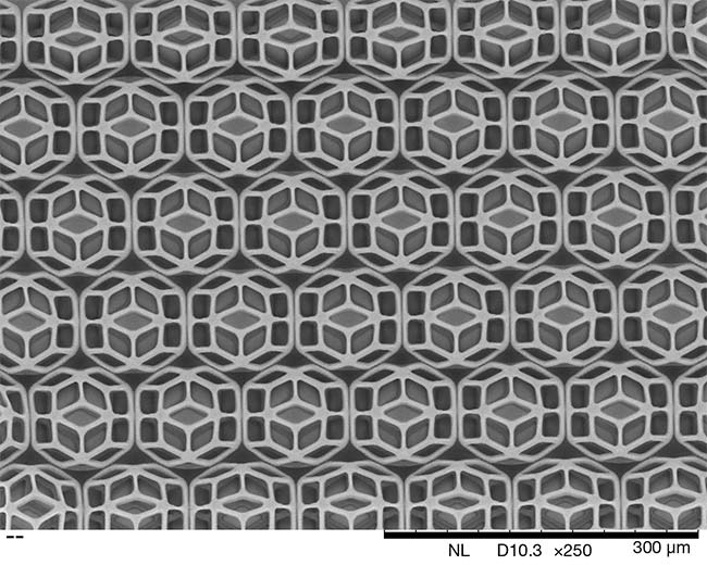
High-numerical-aperture optics focus a femtosecond laser beam into a tiny waist where the peak power of the ultrafast pulses is sufficient to drive two-photon absorption. The additive manufacturing technique delivers submicron spatial resolution and the creation of features as small as 100 nm. Courtesy of Wildman Lab/University of Nottingham.
While SHG and THG microscopy require a femtosecond laser, a continuous-wave laser operating at visible or UV wavelengths can also excite these native fluorophores, but at some expense to depth of imaging and the likelihood of cell damage. So, the advantage of femtosecond excitation is apparent.
Key endogenous fluorophores include
reduced nicotinamide adenine dinucleotide (NADH) and flavin adenine dinucleotide (FAD) — metabolites that can be used as cancer signatures. It has long been known that cancer cells preferentially use glycolysis instead of oxidative phosphorylation to meet their energy needs. This manifests in a distinct difference in the ratio of NADH to FAD
when comparing normal and cancerous cells. NADH is efficiently excited by two-photon absorption at wavelengths between 700 and 800 nm, and the
absorption spectrum for FAD extends to 890 nm.
Early research leveraging these metabolites relied on two different ultrafast laser wavelengths, which is impractical for diagnostic or point-of-care work. Fortunately, in the past couple of years, researchers have shown that a single ultrafast laser operating in the 780- to 800-nm window can excite and image both species with similar efficiency, because NADH’s stronger fluorescence can be excited also at the “red” end of its spectrum. Moreover, the same researchers demonstrated that the NADH/FAD ratio obtained in this way is a reliable marker for two different prostate cancer cell lines2.
Again, the latest compact femtosecond lasers to operate at 780 nm are a good match for this potentially very important application. As with two-photon polymerization, other relevant laser parameters for label-free in vivo imaging include excellent beam quality to maximize spatial resolution, short pulse widths to minimize the average laser power required for fluorescence, and internal power controls to simplify the scanning process — for example, for blanking during raster scanning.
Advanced wafer metrology
Ultrafast lasers are also proving increasingly important in the field of advanced wafer metrology. An established set of techniques, called picosecond laser acoustics (PLA), measures layer thickness and images critical alignment markers under opaque layers. The latter capability is important in multilayer lithography processes.
In the PLA method, the absorption of a laser pulse (i.e., the pump) creates an acoustic wave that travels inward from the laser surface. Underlying layers and structures reflect some of this acoustic energy back to the surface, where it is detected by a change in reflectivity for a second laser pulse (i.e., the probe).
PLA is benefitting from the emerging generation of compact femtosecond lasers because these lasers enable higher-resolution imaging and improved overall measurement.
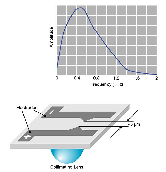
The terahertz radiation produced by ultrashort laser pulses and a photoconductive switch is characterized by high intensity and a broad continuous spectrum. Courtesy of Coherent.
The latest nondestructive wafer metrology method enabled by femtosecond lasers depends on a variant of the harmonic generation process used for the label-free microscopic imaging of cell membranes. The interface between two materials, or any material that is noncentrosymmetric, can generate a small amount of second-harmonic light in a process with a nonlinear dependence on the laser peak power. The SHG light signal can be used to image and detect various features and properties of wafer surfaces and subsurfaces. Such features may include structural defects, film quality, and even trace metal contamination. This technique has been successfully commercialized by FemtoMetrix, a company specializing in optical nonvisual defect metrology for surface, buried, and structural irregularities.
Terahertz generation and detection
Terahertz radiation can deliver unique spectroscopic or imaging information in solid and liquid materials. The low optical frequencies in this range are associated with vibrations of nanoscale particles — for instance, macroscopic molecules such as polymers and proteins, as well as phonon vibrations of extended structures such as crystals. So, terahertz studies are useful to map phase boundaries, as an example. The terahertz frequency range, however, remained a neglected part of the electromagnetic spectrum for decades because there was no easy way to either generate or detect terahertz radiation.
Today, femtosecond laser pulses can be used in several types of mechanisms to generate and detect terahertz radiation.
One method focuses femtosecond laser pulses on a photoconductive antenna (or switch) consisting of a strip of a dielectric material, such as gallium arsenide (GaAs), sandwiched between two metal (e.g., gold) conductors to which a bias voltage is applied. A similar structure is also used as the terahertz detector. Another method to generate terahertz radiation, called optical rectification, focuses the laser into a nonlinear crystal, such as gallium phosphide (GaP) or zinc telluride (ZnTe), to engender difference-frequency generation between different spectral components in the terahertz pulse.
The generation of terahertz pulses via femtosecond laser pulses has several advantages over those generated through continuous-wave methods. The terahertz radiation produced by ultrashort laser pulses has a relatively high intensity. It covers a broad and continuous part of the terahertz spectrum simultaneously, and
its pulsed nature supports analytical techniques, such as time-dependent spectroscopy. As a result, pulsed terahertz radiation is already finding use for imaging applications in such diverse fields as medical diagnosis of cancerous tissue, nondestructive evaluation of pharmaceuticals, identification of explosive hazards, examination of art and archaeology, and defense and security screening tasks.
Terahertz generation via optical rectification can result in high-average-power pulses with a large (frequency) bandwidth if generated by very short pulses from a Ti:sapphire amplifier at 1 to 5 kHz or a nonlinearly broadened ytterbium amplifier at megahertz repetition rates.
Photoconductive antennas, on the contrary, are limited to lower excitation powers due to the potential for optical damage and saturation effects. These antennas, however, are the simplest and least expensive way to produce terahertz pulsed radiation. While most antennas require only 20 to 50 mW of laser power, compact femtosecond lasers emitting single watts at tiled arrays of antennas can achieve higher-power terahertz
generation in a cost-streamlined setup. Such setups, in turn, can potentially broaden the application of terahertz time-domain spectroscopy (TDS) from small laboratory arrangements to larger-scale industrial and medical imaging applications.
How do next-generation femtosecond lasers fit into this terahertz picture? Their short pulse widths enable a broader spectrum of terahertz radiation. Their high average powers centered around 1 W are useful for either method of terahertz generation since they are both inefficient mechanisms that require high input power.
The practical aspects of new femtosecond lasers, such as their streamlined packaging and reliability, are just as important. Some emerging applications need portable or at least transportable systems in order to sustain widespread adoption of these lasers. These small, inexpensive, air-cooled sources that need minimal technical attention can be easily integrated into more complete systems, where they can be mounted in any orientation required.
Future reflections
While femtosecond lasers are often regarded among the most exotic types of coherent sources, their development and application share patterns with all other laser technologies. They have successively transitioned from research subjects to research tools and eventually found use as components within other tools and systems. As with other laser technologies, the evolution of femtosecond sources has been driven by a rapidly expanding field of practical applications spanning from the life sciences to industrial diagnostics to manufacturing processes.
References
1. Q. Geng et al. (2019). Ultrafast multi-focus 3-D nano-fabrication based on two-photon polymerization. Nat Commun, Vol. 10,
No. 2179, www.doi.org/10.1038/s41467-019-10249-2.
2. R. Cao et al. (2020). Multiphoton FLIM imaging of NAD(P)H and FAD with one excitation wavelength. J Biomed Opt, Vol. 25, No. 1, www.doi.org/10.1117/1.jbo.25.1.014510.
Meet the authors
Darryl McCoy is director of product marketing at Coherent Inc., where he manages ultrafast tunable and fiber laser products for nonlinear microscopy and instrumentation markets; email: [email protected].
Marco Arrigoni is director of segment
marketing at Coherent Inc., where he oversees the scientific research and defense markets.
He received a master’s degree in electrical
engineering from Politecnico di Milano.
Arrigoni joined Coherent as an R&D laser engineer in 1988; email: [email protected].