Policymakers and appointed officials outlined many of the U.S. government’s foremost priorities in science and technology, joining with leaders from the photonics sector in Washington, D.C., last week for the second SPIE Photonics Industry Summit. The one-day summit placed a premium on using industry collaboration to help spur economic and technological advancement, with additional focus on workforce development and education.
The event built on last year’s inaugural Industry Summit, which SPIE held six weeks after the CHIPS and Science Act was signed into law. The legislation factored prominently in the program again in 2023, with the road to securing funding under the Chips and Science Act placing high up among attendees’ concerns.
Accelerating and protecting microelectronics growth
Building a strong pipeline to develop and source critical components and technologies remains a central challenge to the U.S.’ chip industry ambitions. At the same time, the need to prevent adversaries from accessing technologies that could pose a national security threat remains top-of-mind for developers and members of government.
This dynamic took the spotlight in the summit’s semiconductor panel discussion, which featured leaders from the National Institute of Standards and Technology (NIST), the Department of Defense (DOD), and the Department of Commerce. The panelists discussed a range of topics that spanned the semiconductor value chain.
Devanand Shenoy, principal director of the Microelectronics Office of the Under Secretary of Defense for Research and Engineering in the DOD, put the aim of the DOD’s Microelectronics Commons network program in the broader context of the department’s approach to bolster the nation’s microelectronics and photonics ecosystem. The Chips Act-funded program aims to enable domestic “lab-to-fab” prototyping for advancements in microelectronics, including electromagnetic warfare, secure computing at the edge and the Internet of Things, AI hardware, and 5G and 6G communications.
Against the backdrop of the DOD’s Sept. 20 announcement that it will award roughly $240 million to eight regional innovation hubs to be part of the Microelectronics Commons network, Shenoy highlighted the potential for lab-to-fab prototyping to bridge the “valley of death” that exists between R&D and production.
“A lot of startups [currently] have to reach outside the country,” Shenoy said. He identified Belgium’s imec as an example of an R&D center that startup American companies have frequently used in turning offshore to demonstrate, scale, or otherwise advance their technology and move toward production.
Panelist Eric Lin, interim CHIPS research and development program director at NIST, pointed to the National Advanced Packaging Manufacturing Program (NAPMP) as another Chips and Science-funded outcome that will support the domestic microelectronics ecosystem.
“There is very little packaging done in the U.S. currently,” Lin said. He highlighted heterogenous integration in packaging as a current technological area of focus and excitement for NIST.
“It is unclear how broad the applications can be,” Lin said, on heterogenous integration. He added that the NAPMP additionally aims to support wafer- and panel-based approaches, substrate technology, and tooling and automation.
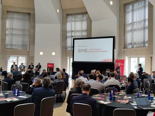
The second SPIE Photonics Industry Summit was held Sept. 27. Industry and government leaders convened in Washington, D.C., to discuss continued industry collaboration, technology advancements, and the impact of science and technology legislation. Courtesy of Photonics Media.
Lin echoed Shenoy about the momentum that the eight forthcoming microelectronics innovation hubs have generated. Standards will be critical to the ability of the ecosystem to advance technology, and they will also play an important role early in the process of getting the hubs up and running, Lin said. It will be the responsibility of each hub to develop sustainable business models and revenue streams. In coordination with other departments, Lin said that NIST will need to ensure that the eight hubs avoid adopting eight different models, which could strain the companies that will ultimately navigate the hubs and use their services.
Matthew Borman, deputy assistant secretary of commerce in the Export Administration Bureau of Industry and Security within the DOD, provided an update on the Department of Commerce’s Bureau of Industry and Security’s so-called Oct. 7 Rule. That order, which was introduced less than a month after the 2022 Industry Summit, placed new export controls on advanced computing and semiconductor manufacturing items to China.
Frontier AI-enabling chips and high-performance compute are areas of ongoing scrutiny from the government. This poses a challenge for technology developers who must continuously monitor and adapt to rules and regulations.
“We know we have to give certainty to industry,” Borman said. He advised that the period after fundamental research has been performed and before wide commercialization takes place is the ideal time to put export controls in place.
Directed-energy roadmap
In a breakdown of the DOD’s directed-energy (DE) roadmap, which included notes on 2024 DE budgets and program budget review, Frank Peterkin, principal director for DE in the Office of the Under Secretary of Defense for Research and Engineering of the DOD, said that science and technology considerations remain dominant for his office. Three successful 300-kW-class demonstrations as part of the DOD’s High Energy Laser Scaling Initiative (HELSI) program were among the recent DE highlights Peterkin cited.
Looking ahead, Peterkin said, while DE source optimization will remain a focus — specifically continuous-wave and pulsed lasers and vacuum tube and solid-state high-powered microwave sources — hypersonic missile defense remains the ultimate priority in U.S. DE. His aim, he said, is to accelerate capabilities related to that undertaking.
To get there, Peterkin identified beam control for advanced threats as a vital area for technological improvement. He said that although the HELSI program will burden DE budgets in the immediate term, he anticipates a budgetary shift toward laser beam control efforts before 2030.
Core messages
Sessions on quantum industry and critical technologies workforce comprised the afternoon portion of the program. U.S. Rep. Joseph Morelle (N.Y) spoke on potential legislative impacts on the photonics industry before the summit concluded with a networking opportunity for guests and speakers.
Again in 2023, the impact of legislation on the industry dominated the day’s dialogue. The recent six-month extension of the U.S.-China science and technology agreement, as well as the potential to reauthorize the National Quantum Initiative Act, for which initial authorization ended last month, factored into sessions on R&D priorities for the fiscal year 2025 budget and quantum, respectively. The state of progress on many of the initiatives introduced by the Chips and Science Act prompted frequent questions and breakout discussions from attendees throughout the day.
In the late afternoon, a focus on the intersection between education and collaboration yielded a highlight moment. Alexis Vogt, endowed chair and professor of optics at Monroe Community College (MCC) and executive director of workforce and higher education at AmeriCOM (the American Center for Optics Manufacturing), shared that the DOD’s Manufacturing Engineering Education Program awarded over $5 million to MCC to fund its optics and photonics associate degree programs. The funding is part of $53 million recently distributed by the National Defense Education Program to 13 organizations.