The packaging around a PIC already contributes to the bulk of its cost. Avoiding these common design mistakes can help improve a design’s performance, robustness, cost-effectiveness, and time to market.
GIJS VAN OUWERKERK, PHIX PHOTONICS ASSEMBLY
We have all heard
that photonic integrated circuits (PICs) can pack a ton of functionality into high-performance, energy-efficient, and low-cost microchips, as well as the promise that they will enable a revolution of powerful optoelectronic devices for a host of applications. However, the complexity of transforming chips into functional
devices is often underestimated and the cost of PIC packaging can take a notoriously big chunk out of the development budget.
Compared to strictly electronic chips, PICs and their packaging are far more complex and not nearly at the same level of maturity and standardization. In addition to needing both electrical and optical interfaces, integrated photonics packaging must deal with a multitude of material platforms — unlike the electronics industry in which CMOS technology has become dominant. PIC platforms such as silicon nitride, indium phosphide, and silicon photonics each have their own strengths and they often benefit from being co-packaged. The packaging costs associated with this complexity can be further inflated by unfavorable choices that are made during the PIC design and layout process.
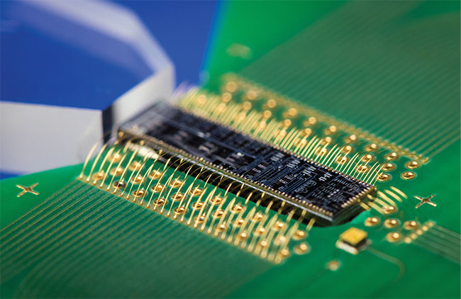
There are numerous ways to deal with dense bond pad configurations on a PIC, including the use of staggered vias to distribute signals to different layers of the PCB. All methods can add significant expense to PIC packaging. But upholding a sufficient bond pad pitch on the PIC can enable the use of a lower-cost PCB, which can offset added packaging costs. Courtesy of PHIX Photonics.
Understanding these easily avoidable mistakes can not only control packaging costs but also promote more effective PIC designs and accelerate the time to market. Importantly, this assumes that the PIC-based module under design is still in the prototype phase. Custom-tailored engineering and manufacturing processes that are only feasible for high-volume manufacturing of frozen PIC designs are not discussed.
There are five common PIC design mistakes that drive up the cost and lead time of PIC packaging by introducing nonrecurring engineering (NRE) steps, complicated manufacturing processes, and the need for high-cost customized components. Avoiding these mistakes can help optoelectronic device designs to better combine performance, robustness, and cost-effectiveness, and pave the way for a smooth scale-up to volume manufacturing.
Favor alignment waveguide loops
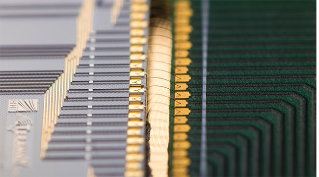
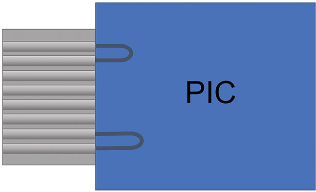
The first common mistake in PIC design is failing to include alignment waveguide loops. Alignment loops, also referred to as optical shunts, are embedded waveguide loops that are not part of the functional optical structures on a photonic chip. They are extra waveguides used for active alignment of the optical interface — commonly between a PIC and a fiber array — during assembly. They allow the packaging foundry to use automated alignment routines with calibrated light sources and detectors. Such routines are similar to the process control monitoring structures used in front-end manufacturing processes. Active alignment is critical for achieving the best possible coupling efficiency for any optical assembly process, save those for high-volume finalized chip designs that are beyond the scope of this article.
It is true that the extra chip area and additional fibers needed for these alignment loops add to the cost of the optoelectronic module. However, let’s look at the consequences of omitting these loops. Without them, active alignment techniques would require the packaging foundry to use probes to activate the functionality of the chip, for example, by driving gain elements and measuring photodiode currents. This approach has a number of disadvantages.
These probes would need to be custom-designed and manufactured and cannot be reused for other projects because they are chip-specific. This would significantly raise the NRE cost of prototype packaging. Incorporating loops postpones the investment in such customized tooling and provides more flexibility regardless of the chip design.
Reliable process control monitoring cannot be performed without waveguide loops because the assembly performance is convoluted with the product performance.
The processes on the chip may be destabilized by the heat and radiation used for epoxy curing during assembly. Reliance on probes makes it difficult to track the waveguide’s position during curing.
The probes may scratch bond pads, making wire bonding more difficult later in the packaging process.
Using functional structures on the chip for alignment requires the packaging foundry to have some knowledge of the chip’s functionality, which may require disclosure of intellectual property that chip designers are not comfortable sharing.
Although waveguide alignment loops occupy space and add some cost to the fiber count, they compensate for this cost by making manufacturing processes much more affordable. They can also help with chip characterization. If the two loops at a fiber array interface are of unequal length, then a first-order estimate of the waveguide propagation loss can be made.
Avoid dense electrical fan-outs
The electrical connections between a PIC and the other components on a printed circuit board (PCB) or housing are typically referred to as the electrical fan-out. For prototype devices, these connections are commonly made using wire bonds. To prevent these wires from shorting or sagging, they should be as short and as parallel as possible. It is therefore advised to make the wire bonds cross over straight from the PIC to the PCB or housing.
The density of bond pads on PICs is limited only by the accuracy of the lithographic etching processes in the fab, which should allow for a very fine pitched electrical interface. And indeed, there is a tendency by PIC designers and PIC foundries alike to put as much functionality onto a given chip area as possible by minimizing bond pad pitches to as low as 70 µm. However, it is often challenging to match that high bond pad density on the surrounding PCB or module housing. Most PCB manufacturers require a bond pad pitch of >200 µm, making a straight crossover from chip to board impossible.
The electrical connections between a prototypical PIC and other PCB components are typically enabled by wire bonds that, to prevent shorting or sagging, should be as short and as parallel as possible. It is advisable, therefore, for these wire bonds to cross over straight from the PIC to the PCB or housing. Courtesy of PHIX Photonics.
There are numerous ways to deal with dense bond pad configurations on a PIC.
One is using a fan-out with high-end thin-film ceramic or organic interposers from a specialized supplier that supports bond pad pitches down to 70 µm.
Another is distributing the bond pads over the entire PIC surface and flip-chipping it onto a land grid array or ball grid array on the PCB. However, this requires redistribution layers and under-bump metallization on the chip, which is rarely available for multiproject wafer services.
Another way is using staggered vias for distributing the signals to different layers of the PCB.
All of these solutions are very expensive due to the higher cost of the components and the NRE steps that they often require. Upholding a sufficient bond pad pitch on the PIC enables the use of a lower-cost PCB that, due to its predictable configuration, can even be a standard stock item at the packaging foundry. This approach will save greatly on the cost and lead time of the package during its prototype stage.
Assign edge allocation wisely
It is highly recommended to avoid
allocating optical connections to adjacent edges of the PIC. The reason is that, in many cases, optical facets need to be polished to enable low-loss butt coupling to other optical components such as fiber arrays and other PICs. Polishing the edges along one side of a PIC requires clamps to be applied to the adjacent edges. This clamping can easily damage previously polished facets on those edges or be hindered by optical components already attached to them.
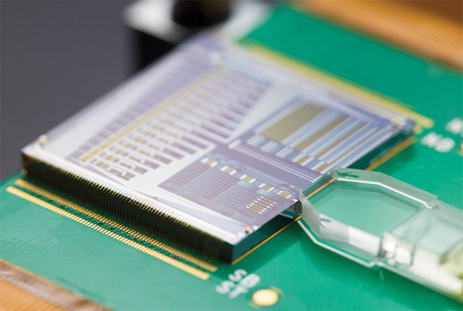
Waveguide alignment loops on a fiber array to PIC interface alignment loops, also referred to as optical shunts, are embedded into a PIC, though they are not part of its functional optical structures. Instead, they allow active alignment of the optical interface, commonly between a PIC and a fiber array, during assembly. Courtesy of PHIX Photonics.
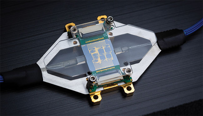
A PIC characterization package in which the north and south edges are allocated to electrical connections and the east and west edges are allocated to optical components. Adhering to a standard allocation such as this allows the packaging foundry to develop standardized housings, PCBs, and assembly processes. Courtesy of PHIX Photonics.
Attaching multiple optical components to a single edge is possible. But their interconnecting waveguides need to be positioned far enough apart to accommodate the size of the components and the tools needed for clamping them during assembly.
Plan for mode field matching
When making optical connections between PICs and, more notably, optical fibers, it is important to consider that there can be significant differences in mode fields between these components. For example, a single-mode fiber for a wavelength of 1550 nm can have a typical mode field diameter (MFD) of 10 µm, whereas in a PIC waveguide the MFD may be <1 µm. Mode field mismatches in either direction cause significant optical losses.
To avoid these losses as much as possible, there are two basic guidelines: The mode fields of two components being coupled together should match as closely as possible, and the matching mode field on the interface should be as large as possible.
One may be inclined to think that if the mode field matches perfectly, its size at the interface is no longer significant. However, small inaccuracies are introduced in the placement of fibers in a V-groove array and during the fiber attachment assembly and epoxy-curing steps. The associated manufacturing
tolerances for these inaccuracies play a greater role as the mode field gets smaller. Therefore, the MFD at the interface should be matched and maximized.
The traditional solutions for mode field matching between fibers and PICs are
to use lensed or tapered fibers with high numerical apertures. Such solutions are preferred for single fiber attachments but pose alignment challenges when applied to multichannel fiber arrays. As dense PICs with high channel counts become the norm, individual fiber treatments are quickly becoming an obsolete solution.
One mode field matching solution that scales well with channel count is the use of spot size converters (SSCs), which taper the waveguide in order to resize and/or reshape the mode field. If the foundry and the PIC platform support it, an SSC can be a functional building block on the PIC itself. On-chip solutions are more affordable and provide the lowest
possible losses, making them highly recommended options. Even in cases in which they cannot completely eliminate mode field differences, on-chip SSCs can minimize them and increase the mode field size at the interface.
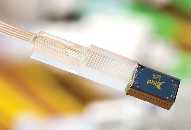
A PHIX silicon nitride spot size converter (SSC) with a configurable mode field is attached to a fiber array. The SSC has configurable input and output mode field sizes, based on how much material is polished away from the optical facets before assembly. Unlike single-fiber mode field solutions, SSCs offer an alternative that scales better with channel count. Courtesy of PHIX Photonics.
A PIC-based lidar module. For low mix/high volume PIC applications, such as lidar, adding extra margin to the chip’s power budget can relax fiber assembly constraints to the point where a more affordable and scalable manufacturing process can be used. Courtesy of PHIX Photonics.
If an on-chip solution is not available or if it does not eliminate the entire mode field mismatch, then it is wise to ask the packaging foundry for options. Foundries such as PHIX, for example, offer SSC interposers pre-attached to a fiber array. These are typically made from ion-exchanged glass or silicon nitride and have lithographically defined tapered waveguides.
Maintain margin in the power budget
Even if the four mistakes listed above
are avoided and a fiber-to-chip interface has been designed for success, it is still important to consider the power budget for this connection. Even the most
optimally butt-coupled fiber-to-chip interface will have some optical losses. But losses can be minimized by enforcing
strict alignment constraints during manufacturing.
Granted, there are markets such as quantum computing that require maximum performance from PICs produced
in low-volume runs, and such markets
are willing to pay a premium for an
additional tenth of a decibel. However,
for less critical PIC applications that scale to high volumes, such as lidar, adding some power budget margin to the module will relax fiber assembly constraints to the point where a more affordable and scalable manufacturing process can be used.
Other parts of the PIC package can also benefit from having some extra margin in the power budget. The need for power budgeting begins with the functional building blocks on the PIC, each of which introduce small losses. For a radio frequency electronic interface between a PIC and a PCB, the packaging foundry will attempt to minimize signal reflections and power transfer inefficiencies by performing impedance matching of the radio frequency trace architecture and wire-bonding scheme. Having a sufficient power margin gives the packaging foundry some freedom to design for manufacturability and cost-effectiveness, instead of focusing purely on achieving peak performance.
Conclusion
Looking closely at the five mistakes discussed in this article, it should become clear that they all share a common cause: focusing the design process too closely on the PIC rather than on the system level. System-level considerations involve the components within the optoelectronic module that the PIC is connected to, such as the fiber arrays, electronics, thermal management solutions, and the housing. System-level considerations also encompass the manufacturing processes used for making these connections, as well as the equipment on which these processes run. A successful PIC packaging foundry leverages all design parameters across multiple disciplines to optimize for the performance, cost, and robustness of the modules.
These five mistakes are just the tip of the iceberg. Make sure to involve your preferred PIC packaging foundry early in the design process. A good foundry partner can help you to not only avoid these mistakes but also define a solid roadmap for your design, from prototype to volume manufacturing.
Meet the author
Gijs van Ouwerkerk, Ph.D., is a marketing and communication specialist at PHIX Photonics
Assembly in Enschede, Netherlands. He cowrote the Design Guidelines for Photonic Integrated Circuit Packaging, available for free download from the PHIX website; email: [email protected].