
SMART Photonics Doubles Production Capacity
SMART Photonics, a foundry for photonic integrated circuits, has scaled up its production of photonic chips by transferring its entire production capability from 3-inch to 4-inch wafer substrates. According to the company, SMART Photonics is among the first photonic integrated circuit foundries offering 4-inch indium phosphide wafer production.
In general, 4-inch wafers contain close to twice the number of chips as 3-inch wafers. The resulting increase in production rate will translate to a lower price-per-chip, the company said.
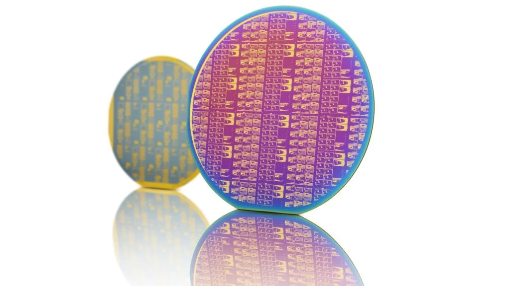
SMART Photonics has transferred its production capability from 3-inch wafers to 4-inch wafers. The larger wafers contain close to double the number of chips as 3-inch wafers. Courtesy of SMART Photonics.
“It’s not just about the sheer number of wafers produced; the larger wafer substrate will now enable us to better meet the number of optical chips needed in the market,” SMART Photonics COO Guy Backner said. He added that the competitive price point will aid the company in its goal to achieve a leading role in the integrated photonics ecosystem.
The transition was enabled in part by a $111 million financing round last year from strategic industry and financial players such as PhotonDelta, chip equipment giant ASML, and chipmaker NXP Semiconductors. The transition also benefitted from the European Union’s Interreg North-West Europe project OIP4NWE.
/Buyers_Guide/Smart_Photonics/c30559