Ultrashort-pulsed lasers are introducing new approaches for fast, cost-effective, and site-specific preparation of samples for microstructure diagnostics in the semiconductor industry.
MANDY GEBHARDT, CLAUDIA RADELOW, AND BORIS ROTTWINKEL, 3D-MICROMAC AG
In recent years, lasers have made significant inroads into analytical applications, such as semiconductor
test and analysis. They are now incorporated into analytical instruments, for example, to detach single atoms from a tiny tip, or to measure a sample’s structure. In semiconductor physical failure analysis (PFA), lasers are used to selectively remove material that encapsulates the die in the semiconductor package to allow for the die to be taken for subsequent analysis — a process known as laser decapsulation. In the last decade, however, laser sources have also made inroads into sample preparation whereby samples are cut and prepared from semiconductor wafers, dies, and packages for microstructure diagnostics and PFA.
Due to the rising costs and complexities associated with scaling advanced lithography, device manufacturers are increasingly turning toward heterogeneous integration techniques that combine and stack different chips and components into advanced packaging architectures, such as 2.5D and 3D integrated circuits. This, in turn, has created new challenges for PFA practices because it is no longer sufficient to remove just one layer or cover in the device or package to isolate the area of interest for microstructure diagnostics. Defects reside deeply within these more complex heterogeneous structures. Manufacturing technology is advancing rapidly, but package analysis techniques need new ways to keep pace.
This has generated increasing demand for sample preparation techniques that can be tuned to various methods of microstructure diagnostics that all need to be fast, reliable, cost-effective, artifact-free, and capable of targeting defects down to the micrometer scale or beyond. Aside from traditional mechanical preparation, focused ion beam (FIB) systems dominate the field. While high costs for skillful personnel and time-consuming processes accompany the former, high ownership costs characterize the latter.
Lasers: an alternative approach
Laser radiation can ablate all kinds of materials, provided that it delivers sufficiently high fluences at the right wavelength. Using ultrashort pulses and extremely high pulse energies, ablation based on multiphoton absorption further enables the machining of materials that are transparent to the laser’s wavelength. Furthermore, laser tools allow very precise positioning of focused beams using standard optical elements. By reducing pulse lengths from a few nanoseconds down to the picosecond or femtosecond range, the material’s ablation becomes increasingly “athermal.” That is, the ultrashort pulses can reduce structural damage from local heating to well below a few microns around the target.
One of the most crucial benefits that lasers offer microstructure diagnostics is that their photons lack any elemental
contamination, or the corpuscular radiation of an ion beam. As a consequence, laser energy will not cause unwanted
implantation effects. Additionally, the ablation rate of laser micromachining is about six orders of magnitude higher than that of a Ga+ FIB used for microstructure
diagnostics sample preparation, and roughly two orders of magnitude higher than the milling rate of a Xe+-plasma-FIB.
Concerns regarding the adverse effects of thermal damage have hampered the wider use of laser micromachining tools for the preparation of microstructure-diagnostics samples. Dominant among these concerns is the potential impact on samples when laser radiation expels matter from the machining location. This occurs because the electromagnetic wave couples to the photonic system and the excitation of photons leads to a local temperature increase.
Laser ablation techniques that employ pulse durations in the pico- and femtosecond range (10−13 to 10−15 s) is often described as cold or athermic ablation. However, this term applies only to pulse durations <10 femtoseconds. Longer pulse durations cause an electron-photon interaction with an associated temperature conduction in the substrate. Ideally, this conduction does not extend beyond a diameter of 100 nm of sample material at pulse durations within the picosecond range.
The advantage of increasingly short laser pulses is their ability to impart all of their laser energy to the material within a short time interval to achieve extremely high-power densities up to a few gigawatts per square centimeter. This leads to very efficient absorption of the laser radiation with minimal thermal damage. Following the fundamental principles of laser micromachining, such as using a low feed rate, can further minimize the extent of the heat-affected zone around a targeted area. Ultimately, the aim is for a specific material layer to contain minimal structural damage (Figure 1). To keep these structural damages minor and under control, a high-precision axis system is also needed to support the laser ablation by allowing for exact positioning of the handled material.
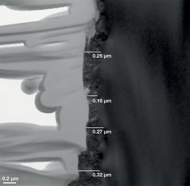
Figure 1. Transmission electron microscopy cross section of laser-micromachined silicon shows the crystallized slabs to be limited to less than a few hundred nanometers. Courtesy of TESCAN ORSAY HOLDING.
As a result of these developments, ultrashort-pulsed lasers are now finding use as “blades” to remove large amounts of material with high precision. Laser tools can cut cross sections easily, making these sections directly usable for further analysis. This has enabled new process routes for preparing sample sizes measuring between several millimeters to a few micrometers. Lasers, for example, can start with the fast removal of large material volumes through the decapsulation phase and follow with the preparation of samples for final processing using a FIB for atom probe tomography or transmission electron microscopy.
Laser-assisted PFA
The semiconductor industry routinely uses PFA to find root-cause failures in electronic components. This practice
helps investigate defects in mobile displays based on organic light-emitting diodes (OLEDs), active matrix-OLEDs (AMOLEDs), and microLEDs. It also helps analyze failure in flip-chip packages, high-bandwidth memory chips, through-silicon-vias, microelectro-mechanical systems, and other microelectronic components. Typical defects leading to failure include cracks, voids, bad contacts, delamination, and underfilled vias.
Sample cross-sectioning is a standard approach in PFA. It allows structures located at different depth planes to be accessible for detailed inspection and analysis using diverse techniques, such as scanning electron microscope (SEM) imaging in combination with energy-dispersive x-ray spectroscopy or electron backscatter diffraction microanalysis.
Cross-sectioning is particularly useful, especially when the regions of interest are situated hundreds of micrometers or a few millimeters below the sample’s surface. This is often the case when dealing with the devices mentioned. However, having
accessibility to the entire surface of such deep cross sections for subsequent inspection requires the removal of large volumes of material of the order of cubic millimeters as well as a precise end-pointing tool that can thin one micrometer layer at a time.
Mechanical sawing, mechanical polishing, and broad ion-beam polishing have been the methods of choice to conduct these tasks in the past. With microelectronic structures becoming increasingly complex and sensitive, other techniques, such as FIB, are increasingly adopted. In general, the superior capabilities of FIB for highly localized sample preparation and precise end-pointing techniques have largely fueled this development. Furthermore, FIB does not induce any mechanical stress on the specimen. As previously discussed, however, FIB is also associated with a high cost of ownership and relatively low throughput.
The increasing demand for electronic devices, along with their miniaturization
and advanced integration, constantly generates the demand for higher volume yields and shorter time-to-result analytical methods, all without compromising quality. The industry cannot rely only on plasma FIB to satisfy such dynamic and challenging needs. The industry needs new approaches for faster and more effective large-volume failure analysis workflows.
The development of large-volume workflows for faster failure analysis of microelectronic devices might combine a stand-alone laser ablation tool with a plasma FIB-SEM system1,2,3. In such a workflow, the laser would begin by quickly removing large volumes of bulk material (Figure 2) followed by plasma FIB-SEM technology performing fine surface polishing. Compared to mechan-
ical sample preparation, this process
significantly benefits from the laser’s end-pointing capability to precisely reach the feature of interest without damaging it.
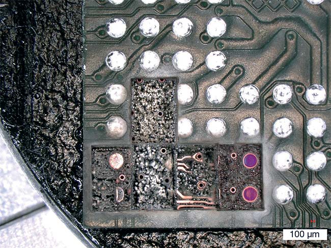
Figure 2. Preparation of a ball-grid array with different laser ablation depths — from the removal of single solder balls to layer-by-layer ablation.
Courtesy of TESCAN ORSAY HOLDING.
In a demonstration of this approach, 3D-Micromac AG and TESCAN prepared a whole 12-mm memory chip to illustrate the long-cuts capability of laser-assisted PFA, as well as the possibility of correcting the taper angle to allow for a perfect alignment of the cross-sectional plane with vertically aligned structures of the device. In the sample, a 1-mm-deep cross section was first prepared to expose hidden structures, such as memory dies located in different layers (Figure 3). Similar workflows can easily deal with preparing large samples and, if needed, prepare them for plasma FIB postprocessing. Long cuts such as these can also cut whole mobile displays, packages, microelectro-mechanical systems, or other large microelectronic components.
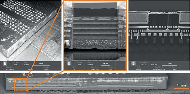
Figure 3. Preparation of a memory stack chip for PFA (above left). Overview of cut memory stacked chip in a stitched scanning electron
microscopy image (bottom). A 1-mm cross
section after plasma FIB polishing supported
by TESCAN’s TRUE X-sectioning kit (above center). The detail of a typical structure after final polishing with Xe+ plasma (above right).
Courtesy of TESCAN ORSAY HOLDING.
Demonstrable improvements
In the demonstration, a laser prepared a 2-mm-wide bulk trench, after which plasma FIB polishing smoothed the cross-sectional wall for subsequent SEM inspection (Figure 4). Cross-sectioning of these types of electronic devices is a common practice that aims to inspect front-end-of-line (transistor active layer) and back-end-of-line (thick metal line) structures as well as solder bumps for defects. Deep cross sections also allow inspection for defects in printed circuit boards. Laser ablation dramatically speeds up the sample preparation time by significantly decreasing the time to prepare the bulk trench, which accounts for most of the preparation time for these cross sections.
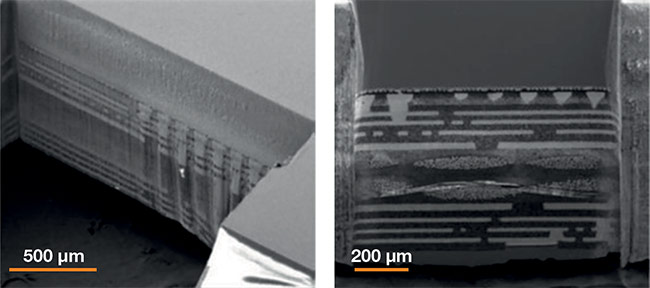
Figure 4. Cross section on a flip-chip package. A 2-mm bulk trench prepared with the laser (left). A 1-mm-wide section polished with a plasma focused ion beam (FIB) (right). Courtesy of TESCAN ORSAY HOLDING.
Advanced preparation techniques
Combining lasers with PFA tools —
such as computed tomography and FIB systems — into correlative workflows makes it possible to navigate through the sample easily and work seamlessly and precisely. In correlative workflows, circuit layouts or image overlays, such as TESCAN’s Large Volume Workflow or Synopsys’ Avalon integration software, can help visualize hidden features. It is possible to mark different locations in these virtual maps of the sample so that each position corresponds to an area in which a cross section needs to be prepared. Locations can be bookmarked on the layout file and saved in dedicated transfer files that can then be loaded on either platform to enable swift navigation of the sample. With a single click, it is possible to find a new region of interest or locations that were previously processed by either tool.
PFA of AMOLED displays is a challenging analytical task in which pairing
laser ablation and plasma FIB can dramatically reduce the time for accessing regions of interest. The typical area of interest in AMOLED displays is the thin-film transistor layers sandwiched between the thick glass substrate and the organic light-emitting active layers (Figure 5). Accessing the thin-film transistor layer requires preparation of cross sections that are hundreds of microns deep, which is highly challenging and time-consuming.
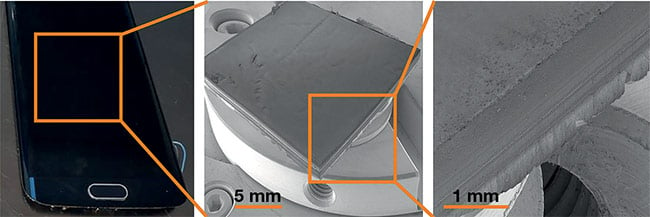
Figure 5. Preparation of active matrix organic light-emitting diode (AMOLED) display samples for physical failure analysis (PFA). Whole AMOLED display to be analyzed (left). A 20 × 20-mm sample extracted from the whole display using laser ablation (center). Detail of one of the side walls of the sample showing no delamination and negligible debris (right). Courtesy of TESCAN ORSAY HOLDING.
Mechanical methods to cut or cleave AMOLED displays can induce extensive damage, such as stress and delamination, that complicates PFA or even makes it unfeasible. With the proper laser parameters, mechanical stress or swelling caused by the laser is negligible, and therefore, no delamination is induced.
The amount of time that is saved by using a laser for sample preparation depends on several factors, including the laser’s power, pulse energy, and power density, as well as the ablation rate of the material. In the case of the examples
demonstrated above, preparation and analysis took 60% to 70% less time
in comparison to conventional FIB
approaches.
Further experiments conducted by 3D-Micromac using a newer laser source have demonstrated that sample preparation time can be shortened further. This enables the possibility of sample preparation applications that would otherwise not be economical due to high time expenditure.
Conclusions
Ultrashort-pulsed lasers generate new approaches for fast, cost-effective, and site-specific preparation of samples for microstructure diagnostics in the semiconductor industry. In combination with other analysis techniques, correlative working approaches can also be used to process and expose hidden areas with
the aim of significantly accelerating PFA. A laser micromachining system is the ideal equipment with which to perform various tasks in microstructure diagnostics at any time.
Meet the authors
Mandy Gebhardt studied business administration/business information technology at the University of Corporate Education Glauchau in Germany. Mandy joined 3D-Micromac in 2006. Since then, she has been responsible for marketing communications and public relations.
Claudia Radelow studied media manage-
ment and industrial management at the
University of Applied Sciences Mittweida in Germany. Claudia joined 3D-Micromac in 2019 and is working as product marketing manager and focusing on microdiagnostics.
Boris Arnold Rottwinkel began his engineering career at Friedrich-Alexander-University Erlangen-Nuremberg in Germany in materials science and engineering. From the University of Technology Clausthal-Zellerfeld he received his Ph.D. in mechanical engineering. In 2018, he joined 3D-Micromac as sales and product manager for microdiagnostics.
Acknowledgments
The authors wish to thank Rodrigo Delgadillo Blando, Lukáš Hladík, and Jozef Vincenc Obona from TESCAN ORSAY HOLDING a.s. for supporting the sample preparation and providing the images and results shown in the papers cited in the references.
References
1. R. Blando, L. Hladík, et al. (2021). Pairing laser ablation and Xe-plasma FIB-SEM: An approach for precise endpointing in large-scale physical failure analysis in the semiconductor industry. Presented at ISTFA Conference Proceedings.
2. M. Tucek, R. Blando, et al. (2020). Speeding up large-scale failure analysis of semiconductor devices by laser ablation. Presented at ISTFA Conference Proceedings.
3. M. Tucek, M. Búran, et al. (2020). Laser ablation for throughput increase in large volume semiconductor failure analysis tasks. Presented at ISTFA Conference Proceedings.