About This Webinar
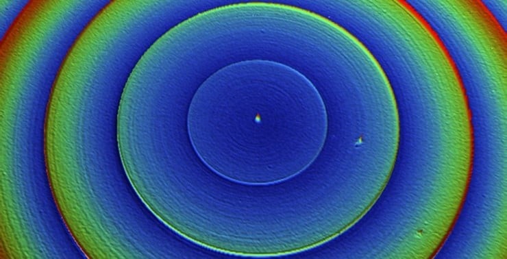
Microlenses are critical components used in a wide variety of consumer devices and industrial sensors, ranging from cellphone cameras and virtual reality goggles to 3D displays and advanced driver-assistance systems. Simple lenses have a fixed radius of curvature, but more complex aspheric shapes provide sharper focusing, less distortion, and astigmatism correction. Other design advancements include arrays of microlenses that can focus light from large fields of view to individual pixels on a CMOS camera, and a Fresnel microlens that can minimize chromatic aberration. Usually ranging in sizes from a millimeter to a few microns in diameter, microlenses, including complex ones, are produced in large volumes. Since microroughness and geometry factors directly affect performance, high-throughput metrology control of microlenses is critical for lens development, process optimization, and mass production within tolerances.
Roger Posusta of Bruker Nano Inc. discusses how white light interferometry (WLI) has the capability to encompass several lenses in a large field of view while maintaining subnanometer height resolution and micron-level lateral resolution. WLI is an ideal optical measurement technique for characterizing these types of surfaces. Bruker’s industry-leading WLI solutions combine automation and on-the-fly analysis to enable comprehensive reports on lens parameters. Posusta also covers curvature analysis through the Zernike coefficient, defect monitoring via slope-based detection, and deviation from ideal aspheric shape. Finally, he illustrates the calculation of the conic parameter using automatic lens shape detection, which enables the high-throughput and advanced characterization of the most complex microlenses.
Who should attend:
R&D scientists, engineers, manufacturers, and educators who utilize microlenses. Those in industries such as aerospace, automotive, communications, energy, medicine, nanotechnology, ophthalmology, and semiconductors who are interested in white light interferometry. Anyone who works with technologies such as coatings, sensors, displays, imaging, microscopy, nanophotonics, and test and measurement.
About the presenter:

Roger Posusta is a senior marketing application specialist at Bruker Nano Inc. He has over 35 years of experience helping industry and academia implement noncontact metrology solutions to solve their most challenging applications.
About Bruker:
Bruker’s high-performance scientific instruments and high-value analytical and diagnostic solutions enable researchers and engineers to explore life and materials at nano-, micro-, and macroscales. In close cooperation with their customers, Bruker is enabling innovation, improved productivity, and customer success in the life sciences, materials, and industrial applications.