 3D Scanning Method Captures Fast-Moving Objects Without Motion Artifacts
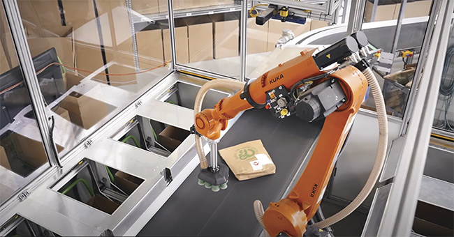
Logistics can spell the difference between success and failure in business. Receiving, storing, inspecting, sorting, packaging, labeling, shipping — all of these steps need to happen quickly to...
Vision Spectra Autumn 2022 Issue