About This Webinar
Photonic integrated circuits (PICs) are currently fabricated primarily in CMOS semiconductor fabrication facilities, which allows manufacturers to take advantage of the large installed base of tools and processes. However, for a variety of reasons, traditional electronic packaging—which is the final step in the manufacturing process—is not equipped to handle the inherent challenges associated with packaging these advanced devices into functional products. In this presentation we explore some of these challenges, such as sub-micron alignment tolerances, sensitivity to temperature variations, optical losses, and a lack of established standards, especially as they relate to the design and manufacture of optical coupling structures.
Harame and the team at AIM Photonics learned that the best results are obtained when the PIC manufacturing and packaging processes are co-designed to better achieve low-loss coupling, particularly between photonic integrated circuits and other elements in the system. AIM’s “end-to-end” approach to developing an integrated photonics manufacturing ecosystem—including electronic photonic design automation (EPDA), wafer manufacturing (including interposers and heterogeneous integration), and electronic-photonic test, assembly, and packaging capabilities—enables the development of reliable, accessible, and affordable solutions that ensure the manufacturing-readiness of this critical technology for decades to come.
*** This presentation premiered during the
2024 Photonics Spectra Integrated Photonics Summit. For more information on Photonics Media conferences and summits, visit
events.photonics.com.
About the presenter
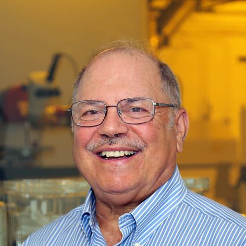
David Harame, Ph.D., is the associate vice president for EPDA, test & packaging, and process development for New York CREATES and the Chief Operating Officer for AIM Photonics. He is responsible for the organization’s photonic technologies, heterogeneous integration, electronic photonic design automation process design kits, and Test, Assembly and Packaging (TAP) operations in Albany and Rochester, N.Y. Harame is an IEEE Fellow and has held numerous other industry leadership roles throughout his career after earning his doctorate in electrical and electronics engineering at Stanford University.