The University of Pennsylvania’s (Penn) Agarwal Group, headed by professor Ritesh Agarwal, seeks to understand how light interacts with small-scale nanostructures. The group then uses that understanding to engineer useful and innovative optoelectronic devices.
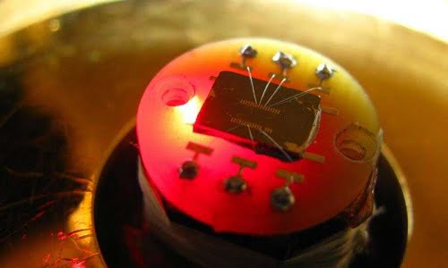
A silicon-based photonic device that is sensitive to the spin of the photons in a laser shined on one of its electrodes. Light that is polarized clockwise causes current to flow in one direction, while counter-clockwise polarized light makes it flow in the other direction. Courtesy of University of Pennsylvania.
One area the researchers at Penn’s Department of Materials Science and Engineering is focusing on is photon “spintronics,” a variation of electron-based spintronics but applied to measuring photon spin for applications in optical devices and circuits.
“Current electronic devices work by measuring the number of electrons that flow in a circuit. In spintronics, the idea is to encode more information in electron spin,” Agarwal said. “Analogously, if we can engineer properties of materials via an interplay of symmetry, geometry, and topology, then we can encode more information in photon spin. Recently, by using materials called topological Weyl semimetals, we were able to detect on-chip the spin of the photon, and the next step we are currently working on is to also design photodetectors sensitive to what are called the orbital angular degrees of freedom of light.”
Agarwal told Photonics Media that the idea behind the photon spin is to encode and extract more information in optical circuits.
“We showed that even in a material like silicon, which has all the mirror symmetries, we can still make the material chiral by engineering its geometrical properties,” he said. “For example, by cutting the material in a particular direction, by applying electrical fields, we broke all the mirror symmetries in silicon. By doing so we were able to detect the photon spin using Si, a workhorse material for electronics and photonics.”
The Penn researchers’ focus with photon spin is to make silicon photonics work at the same length scales as silicon-based electronics.
In a typical computer chip that is opened up, there are features that are 20 to 40 nanometers in diameter; these are basically silicon based electronic transistors. However, to make optical devices that are comparable to the size of the optical wavelength, they have to be many microns in size.
“If you want to integrate electronics with photonics, and your optical devices are two or three orders of magnitude larger in size than your electronics, then there is a size mismatch,” Agarwal said. “What we’ve been trying to focus on is trying to reduce the length scale of silicon-based photonics down to tens of nanometers.”
The Agarwal Group has created silicon-based detectors that can detect photon spin very reliably and with very high fidelity. They’re also trying to make modulators and silicon-based Raman lasers at the same length scale as silicon-based electronic devices. The researchers say they can extend the same idea of photon spin in commercial silicon-based single-photon detectors and make them sensitive to photon spin.
The Agarwal Group is also working to understand and engineer light-matter interactions in atomically thin materials called two-dimensional semiconductors. Other research areas include nanoscale phase change electronics and photonics.
For more on the Agarwal Group, watch the latest episode of Light Matters.