A shift in assembly methods would help reduce costs and increase production in the optoelectronics manufacturing and packaging industries.
Bruce W. Hueners and Michael K. Formica, Palomar Technologies
Manufacturing the laser diode is complicated by the existence of multiple proprietary techniques and intellectual property barriers together with complex device physics and unique materials.
Process engineering, design for manufacturing, design for test, standardization, outsourcing and automation are common procedures in other high-technology industries but remain largely absent in photonics. A better understanding of these processes will enable manufacturers to optimize yields by confronting cost barriers and other obstacles with new assembly methods, where appropriate.
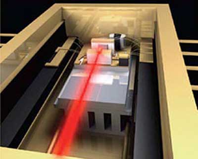
Figure 1. Photonic device packaging.
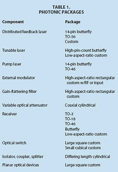
Today, standardizing photonic package configuration is critical (Figure 1). Device functionality dictates format. High-performance devices are generally assembled in butterfly packages, while lower performance devices go in lower cost packages. Packaging accounts for 60 to 80 percent of the cost of a photonic component, compared with 20 to 30 percent in the semiconductor industry. Considering the many packaging methods employed in the construction of various photonic devices, such as those outlined in Table 1, it becomes clear that these methods require custom manufacturing equipment and processes.
 Moreover, such devices are electronic/photonic hybrids with a variety of unique materials used in their fabrication — a factor that distinguishes optoelectronic device assembly from conventional microelectronics. From a variety of materials — notably silicon, quartz, doped silica, lithium niobate, gallium arsenide and indium phosphide — component manufacturers select the most appropriate for the specific device, and each device is discrete from the rest of the optical circuit (Figure 2), although this is changing with the advent of photonic integrated circuits.
The drive to reduce size, power consumption and cost encourages the development of optical integrated circuits. This presents new challenges for component manufacturing, including determining which materials are best for which components. For example, in high-speed data transmission systems, the source laser is modulated with a lithium-niobate external modulator.
However, because lithium niobate is not suitable for use as a laser source, it is difficult to integrate the modulator and the laser. As a result, modulators manufactured from gallium arsenide and indium phosphide, both of which are suitable laser materials, are being introduced.
Every step is important
From chip fabrication to coating to testing, each step involved in manufacturing a laser diode is important. Each step generates yield loss and scrap — ultimately resulting in more costly finished products. The key cost-reduction strategy in the semiconductor industry is "no forward defects," as each serial process step adds value to the finished product.
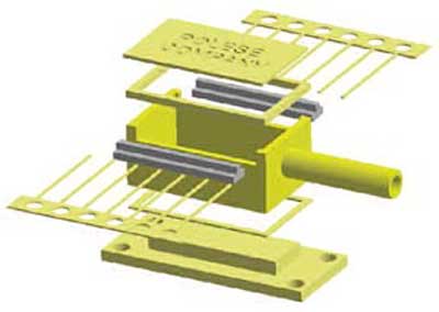
Figure 2. Typical package configuration features a built-in heat sink, a port for optical fiber and leads for mounting the assembly on a circuit board. Courtesy of Polese Co.
A substrate crystal orientation of (001) is essential for producing laser diodes because the manufacturer should produce the parallel mirrors by cleaving the wafer in the (110) plane that is normal to the (001) crystal plane. Grooves 50 μm deep are fabricated photolithographically with a spacing of approximately 200 to 300 μm in the wafer to provide scoring lines for chip singulation. Normally, the wafers are polished from the back side to a thickness of approximately 100 μm.
Next, the wafer is cleaved along the direction normal to the grooves in the wafer. Special care must be taken to prevent the introduction of defects, such as dislocations from the chip edges to the inner crystal caused by surface damage during cleaving. In this stage, each diode is tested under pulsed operation, and good devices are selected.
After cleaving the wafer into diode arrays or bars, a protective dielectric film such as SiO2, Al2O3 or Si3N4 is deposited by RF sputtering or chemical vapor deposition on both mirrors of the waveguide’s facets. The mirror’s surface is protected from atmospheric exposure to suppress oxidation of the facets, which causes long-term degradation, and to reduce surface recombination velocity, which is an important parameter for catastrophic failure.
During device fabrication, external stress also may be applied to the diodes. When cleaving processed wafers into diode arrays, mechanical damage may be induced from the cleaved edge of the crystal, generating dislocations in some cases. Moreover, during the die attach or wire bonding step, thermal or mechanical stress may accumulate elastic strain in the diode or may generate mechanical damage or scratches in the crystal. To minimize stress and to enable extremely repeatable and consistent results, this process should be automated and programmably-driven.
Consider the attachment of a laser diode within a source or pump laser. This is an extremely temperature-sensitive device that requires careful process control during assembly. Precision eutectic component attach includes pick and place of the silicon, gallium-arsenide or indium-phosphide chips; in situ reflow of the preform or pretinned devices in concert with programmable
X-, Y- or Z-axis agitation; and programmable pulse heating or steady-state temperature.
The reflow profile during an in situ eutectic die attach process is engineered to provide consistent melting and a void-free attach interface. The resulting heat transfer from the laser diode contributes significantly to temperature stabilization during laser operation (Figure 3).
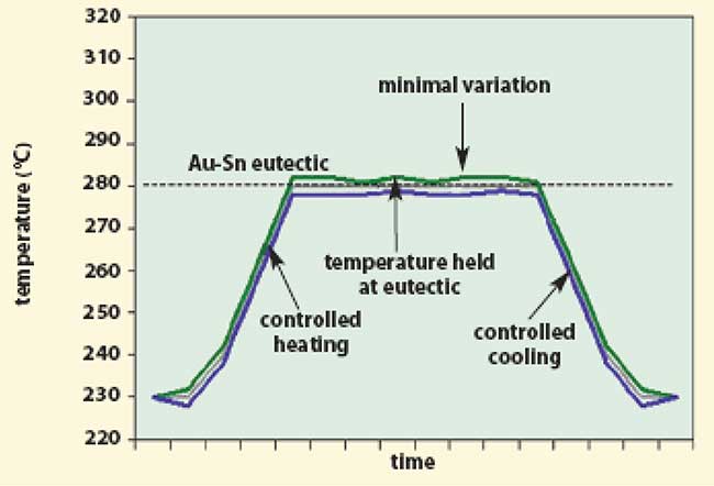
Figure 3. Reflow profile of a laser diode module assembly.
Align and attach
The final assembly step is to align and attach an optical fiber. To optimize the coupling efficiency, especially with single-mode devices, final alignment must be made to within 0.1 μm of the actual peak. Because of manufacturing variances in the diode, diode assembly and optical fiber core center, the fiber must be actively aligned.
This typically is performed before the fiber or array of fibers is permanently attached to the device by laser weld, solder or epoxy. The feedback from or induced by the device being placed determines the optimal position of the optical component.
Alignment occurs in all six degrees of freedom: the X-, Y- and Z-directions, pitch, roll and yaw. The most common metric employed is optical power, which may be based on other parameters, such as polarization.
The most critical parameter from any attach system is the final, postattach optical power. This process may induce stress or mechanical shift for which the system must account. Even a submicron shift may render a device useless, so careful control of the fiber align and attach process is essential.
One common set of measurements that offers insight into chip attach integrity is the light-current-voltage (LIV) test. In it, the drive current through the laser is ramped from zero to the maximum operating current, and the output power of the laser and the forward voltage across the diode junction are recorded.
Comparing the continuous-wave (CW) and pulsed current curves gives an indication of the diode attach integrity. If the heat flow through the die bond is high, the two curves will be similar. If the bond is flawed, however, the heat flow will be low, the laser chip will heat up during CW operation, and the two curves will be substantially different.
A more quantitative measure of the die bond efficacy can be obtained by understanding that several characteristics of laser diodes depend on the junction temperature; e.g., output power, forward voltage, wavelength and threshold current. The most straightforward quantitative testing method involves measuring the laser’s wavelength, which enables a calculation of the thermal impedance, a direct measurement of the chip attach quality.
During LIV testing, the laser diode module is characterized at various drive current levels. Typically, these tests are run on a dedicated, computer-controlled test stand containing current and voltage sources, an instrument to power and control the thermoelectric cooler inside the module, one or more photodetectors or other sensors, and sensitive current measurement capability. These instruments typically are integrated into an LIV test system that generates plots of the relationship of the light output, the drive current and the voltage characteristics of the laser diode module.
The functional requirements of a typical LIV test system include high-precision current sourcing to drive the laser diode, the ability to measure subpicoamp currents at femtoamp-level resolution and the control of the thermoelectric cooler that regulates the operating temperature of the module. Temperature control to ±0.01 °C is necessary to ensure consistent wavelength output from the module and to protect the device from damage caused by overheating.
Putting it all together
The optoelectronic component manufacturing and packaging industry is under considerable pressure to reduce costs. Most manufacturers have recognized that a shift in assembly methods will help drive down component costs and accelerate the rate of production.
This has sparked a move away from the manual assembly processes that have characterized the industry for decades to high-accuracy, high-yield, automated methods. In addition, more suppliers who can support the stringent tolerances and the great variety of products are emerging. The equipment and process expertise that these suppliers are developing not only will make the manufacture of optical components more efficient, but also will enable component designers to push the envelope of communications technology into the future.