An examination of the packaging technology of photonic components for optical communication and other areas of photonics.
Torsten Wipiejewski, VNT Management Oy, German Office
Photonic components are key elements for the information technology (IT). Photonics technology covers the generation of information (cameras, sensors), its transportation (optical communication), storage (CD, DVD) and display (CRT, LCD, others).
The high bandwidth and low attenuation of silica optical fiber enables long-distance phone calls and high-speed Internet access with almost no limits at very low cost. In fact, downloading data from the Internet is basically free, because the optical fiber infrastructure is efficient and requires minimal maintenance.
In the new millennium, photonic applications have emerged in the automotive, industrial control, consumer electronics and home networking arenas. Almost four million cars are produced every year that contain infotainment systems based on an optical network. The advancement and spreading of digital entertainment devices (digital TV, DVD, video games) drives the installation of high-bandwidth optical links into the home environment.
Optical communication systems
Optical long-haul telecom systems have been in service since the 1980s. The 1990s saw tremendous growth in the optical datacom market. In the new millennium, bitcom systems are emerging that are characterized by very short distance optical interconnects with distances in the range of meters or tens of meters. Figure 1 provides an overview of different layers of optical communication systems.
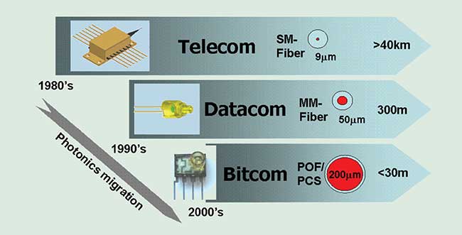
Figure 1. Migration of photonics from telecom to datacom to bitcom. Telecom systems use single-mode (SM) optical fiber for highest performance, datacom systems use multimode (MM) fiber for short range in order to relax alignment tolerance, thereby reducing cost, and bitcom systems achieve further cost reduction of optical components and connectors by increasing the fiber core diameter to 0.2 mm or more.
New communications technology is driven by the desire to decrease the cost of information transportation. In order to achieve this goal we can reduce the cost of components or transport more bits per length of time (higher speed) or transport information over greater distances without the conversion back to electrical signals. This is the key strategy for telecom systems. For a given distance and/or required transmission data rate, we can only reduce the component cost to minimize the total system cost. This is especially true in short-distance systems and data aggregation or distribution networks like fiber-to-the-home. Options for component cost reduction are: integration of electrical components, integration of optical components, use of lower cost material, and reduction of manufacturing cost (e.g., by automation). On-going cost reduction enables new applications for optical fiber systems where cost was previously prohibitive.
Telecom components
Telecom systems are designed for high bit rate and long distance. Therefore such systems employ single-mode fibers. The operating temperature range is typically 0 °C to +70 °C. The operating wavelength is primarily around 1550 nm, the loss minimum of silica fiber. For the transmitter and receiver side of the optical communication link, we can consider different layers of packaging as listed in Table 1.
TABLE 1.
LAYERS OF PACKAGING FOR AN OPTICAL FIBER TELECOM SYSTEM
| |
|
Component
|
|
Remark
|
| |
|
|
|
|
| Layer 0 |
|
Opto chip |
|
Laser, photodiode |
| |
|
|
|
|
| Layer 1 |
|
Chip on carrier |
|
Laser chip on a substrate for testing
and mounting |
| |
|
|
|
|
Layer 2
|
|
Component package
|
|
Transmitter: hermetic butterfly-style
package containing laser, optical
components, thermoelectric cooler,
optical fiber pigtail
Receiver: hermetic butterfly-style
package containing photodetector,
optical components, optical fiber
pigtail
|
| |
|
|
|
|
Layer 3
|
|
Line card
|
|
Transmitter and receiver butterfly
packages, optical multiplexer
components, monitoring
components, electronics circuits
|
| |
|
|
|
|
Layer 4
|
|
Rack |
|
Several line cards, optical amplifier
cards, electronic switching cards,
client-side communication cards
|
In this article we will discuss only features up to the component package layer. Figure 2 shows a typical butterfly-style package in a cross-sectional view. The package consists of metal, typically Kovar. An optical fiber pigtail is attached to one of the front-end sides. Electrical leads feed through the sidewalls of the package. The electrical traces are embedded in ceramic material for electrical isolation. The electrical impedance matching of the feedthrough becomes a challenge at high frequencies for applications above a data rate of 10 Gb/s.
Inside the transmitter package is the chip carrier with the laser chip mounted on it. A thermistor is mounted on the same carrier to track the temperature of the laser. The thermistor signal is used in the external control circuit as a feedback signal to adjust the power of the thermoelectric cooler (TEC) at the base of the package. The TEC stabilizes the laser temperature, typically within ±1 °C or less. The temperature stability requirement is determined by the specification for the emission wavelength of the transmitter, since the temperature determines the emission wavelength of the laser. For dense wavelength division multiplexing (DWDM) applications, the required wavelength accuracy is typically 5 GHz in a system with 50 GHz channel spacing.
A monitor photodiode is mounted facing the back facet of the laser chip for output power control. The signal from the monitor photodiode is used by the external control circuit to adjust the laser current. The typical requirement for output power stability is less than 0.5 dB over temperature and lifetime. Sometimes the monitor photodiode is placed at the front side. In this case, a portion of the output light beam is tapped off with a semi-transparent mirror and directed onto the monitor photodiode.
The laser emission is collimated by a lens mounted close to the laser facet. The lens is typically an aspheric glass lens with a relatively high numerical aperture to capture most of the light from the laser. Since the laser output beam is quite elliptical with a larger divergence angle in the vertical than in the horizontal direction, the coupling efficiency into the single-mode fiber is limited to about 50 percent. The collimated laser beam travels through an optical isolator before being coupled into the fiber. The optical isolator is necessary for distributed feedback (DFB) lasers. It prevents light of parasitic reflections from re-entering the laser cavity. Without an isolator, the DFB laser emission can become very noisy and the optical system does not operate well.
Additional elements can be inserted in the optical path next to the optical isolator. In DWDM applications this could include an integrated wavelength locker. This device measures the optical emission wavelength of the laser and provides a feedback signal to the external control electronics to adjust the laser temperature or a laser tuning current in the case of a tunable laser.
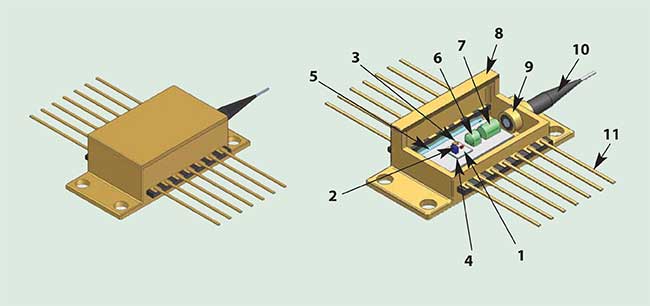
Figure 2. Butterfly package for telecom applications showing the laser chip (1), monitor photodiode (2), thermistor (3), chip carrier (4), thermoelectric cooler (5), lens (6), optical isolator (7), component package (8), window for light output (9), fiber pigtail (10) and electrical leads (11).
The butterfly package shown in Figure 2 features a window in the package wall for light output. A lens can be integrated in the window for improved coupling of the light into the fiber pigtail outside the package. In other package designs, the fiber end is inserted into the package through the package wall. In this case, the silica fiber is first metallized and then soldered to a metal feedthrough tube in the package wall. The solder process provides the necessary hermetic sealing.
Butterfly assembly process
The butterfly laser assembly process uses mostly soldering processes. First, the laser chip is soldered on the carrier, then the carrier on the thermoelectric cooler. Finally, everything is soldered to the base plate of the butterfly package. The solder processes follow a certain hierachy where solders of higher melting temperature are used first to avoid remelting of solder joints.
The mounting of the first optical lens requires active optical alignment. The lens is positioned in X-Y-Z directions with micropositioning units and fixed in place by laser welding. The butterfly package is closed with a lid. The lid attachment is a seam-seal electrical welding process. Prior to seam-seal, small amounts of helium are added to the atmosphere inside the butterfly package. Any leakage of the package can be detected in a helium leak tester. The optical fiber pigtail is also actively aligned and fixed in position by laser welding.
Epoxy material is seldom used in butterfly packages because of outgassing concerns. If they are used they have to be selected carefully in order to meet the stringent requirements for components used in telecom systems. Outgassing material can potentially condense on elements in the optical path and thereby change output power or cause other reliability issues.
Datacom components
Datacom components are used for computer interconnects, telecom switching equipment and other applications. The operating wavelength of datacom transceivers depends on the link distance. For distances up to several hundred meters, multimode silica fibers are employed because their larger core diameter relaxes mechanical alignment tolerances, thereby reducing the cost of optical components such as coupling units and connectors. For distances up to 2 km, 1300 nm Fabry-Perot lasers and single-mode fibers are the right choice. For up to 15 km, 1300 nm DFB lasers are employed because of the lower dispersion penalty. Beyond 15 km, 1550 nm DFB lasers are used in order to match the low attenuation window of silica optical fiber.
TABLE 2.
LAYERS OF PACKAGING FOR DATACOM TRANSCEIVER MODULES
| |
|
Component |
|
Remark |
| |
|
|
|
|
| Layer 0 |
|
Opto chip |
|
Laser, photodiode |
| |
|
|
|
|
Layer 1
|
|
Component package
|
|
Transmitter side: laser chip with
monitor photodiode in TO-can
Receiver side: photodiode and
transimpedance amplifier in TO-can
|
| |
|
|
|
|
Layer 2
|
|
Optical subassembly
|
|
TO-can with optically aligned barrel
for fiber coupling
Transmitter side: transmitter optical
subassembly (TOSA)
Receiver side: receiver optical
subassembly (ROSA)
|
| |
|
|
|
|
Layer 3
|
|
Optical module
|
|
Transceiver module package with
TOSA, ROSA and postamplifier, and
some other electronics to provide
standard electrical interface
|
Datacom products are typically sold as transceiver modules including the transmit and receive elements plus some electronic circuits to provide a standard electrical interface. If a multiplexer function is included, the modules are called transponders. 10 Gb/s modules are mostly transponders; at 2.5 Gb/s or below they are primarily transceivers. Small-form-factor (SFF) transceivers of 0.5 × 0.39 × 2 in. are the most common. Sometimes they can be plugged and unplugged while the system is powered up (hot-pluggable), in which case they are called SFP transceiver modules. The normal operating temperature range of datacom modules is 0 °C to +85 °C. Table 2 lists the different layers for the packaging of the components for a typical transceiver module.
The transistor outline can (TO-can) is the standard package for datacom components. It was originally developed for transistor packaging and is widely used for optoelectronic chips. Most CD and DVD lasers are packaged in TO-cans. The TO-can provides hermetic sealing of the chip and is relatively inexpensive because of the huge manufacturing volume.
Figure 3 shows a TO-46 package with an attached plastic barrel for coupling to a multimode optical fiber. The speed of TO-cans is normally sufficient for applications up to 2.5 Gb/s. However, TO-cans with an improved impedance matching at the electrical feedthroughs can operate at 10 Gb/s.
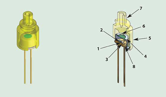
Figure 3. TO-can package for datacom applications showing the VCSEL (1), monitor photodiode (2), submount (3), flat window cap (4), plastic barrel (5), plastic lens (6), barrel for connection to a fiber ferrule (7) and electrical feedthroughs (8).
Many modifications exist to the example shown in Figure 3. The TO-can provides a basis for the mounting of the optoelectronics chip. For the transmitter side, 850-nm VCSELs are used for most multimode fiber links. Next to the VCSEL is a monitor photodiode for automatic output power control. Sometimes the VCSEL and the monitor photodiode are mounted on an additional submount. The VCSEL light is emitted through a flat window cap and focused into the fiber with a plastic lens. The window cap reflects some of the VCSEL light onto the monitor photodiode. Therefore the photo-current is proportional to the VCSEL light output. The plastic molded part contains the focusing lens and a barrel feature for a mechanically stable connection to the fiber ferrule.
TO-can assembly process
The manufacturing process starts with mounting the VCSEL, monitor photodiode and submount on the TO-header. The window cap is attached in an electrowelding process. With the cap, the TO-can is hermetically sealed. Most diode lasers are shipped in this format. Afterward the barrel is optically aligned in X-Y-Z direction relative to the TO-can using active alignment. The VCSEL operates at some nominal current and output power. The barrel is fixed with UV epoxy and later cured. This component including the TO-can and the barrel is called the transmitter optical subassembly (TOSA).
On the receiver side, the components inside the TO-can are the photodetector and the first stage transimpedance amplifier. Sometimes additional capacitors are also included. The assembly process is equivalent to the transmitter side. The TO-can with the attached barrel is called the receiver optical subassembly (ROSA).
For single-mode applications, the alignment tolerances are much tighter compared with the multimode system. Since the fiber core diameter is approximately 9 µm, the mechanical precision needs to be within 1 µm. Therefore the barrel is typically made of stainless steel. The coupling lens is made of glass or sapphire and inserted into the barrel. The optical alignment is fixed using a laser welding process for the X-Y-Z direction.
The TO-can contains a vertical stem for the mounting of the edge emitting laser. The back facet of the laser chip looks toward the bottom of the package. The monitor photodiode is mounted at this position. The emission from the front facet is coupled to the single-mode fiber. The mounting of the laser chip requires wire bonding at a 90° angle. In the case of DFB lasers, an optical isolator is also inserted into the metal barrel.
Bitcom components
Bitcom components are for applications using large-core optical fibers. The emphasis is on low cost to compete with electrical wiring solutions. To reduce cost, bitcom systems are designed for large mechanical alignment tolerances. Polymer-clad silica (PCS or HCS) fibers or plastic optical fibers (POF) with large core diameters of 200 µm to 1 mm are used. These fibers relax the alignment and manufacturing tolerances of optical connectors compared with multimode (50 µm core diameter) or single-mode (9 µm core diameter) fibers. In addition to their high speed potential, bitcom optical links beat electrical links in respect to electromagnetic interference (EMI) noise generation and immunity to EMI. They are also smaller, more flexible and lighter weight compared with high-speed copper cables such as shielded twisted pair (STP) or coaxial. This makes optical fibers the preferred communication media in automotive applications even at data rates of only 25 Mb/s.
TABLE 3.
LAYERS OF PACKAGING FOR BITCOM MODULES
| |
|
Component |
|
Remark |
| |
|
|
|
|
| Layer 0 |
|
Opto chip |
|
Laser, photodiode |
| |
|
|
|
|
Layer 1
|
|
Component package
|
|
Transmitter: laser chip and driver IC
chip, sometimes with monitor
photodiode
Receiver side: photodiode and
transimpedance amplifier,
sometimes with postamplifier
|
The operating wavelength of bitcom components depends on the fiber type. For plastic optical fibers based on PMMA material, the normal transmission window is around either 650 or 520 nm. The transmitter light sources are LEDs or resonant cavity LEDs (RECLED). RECLEDs can provide higher speed than LEDs up to 250 Mb/s. For polymer-clad silica (PCS) fiber, the transmission window includes 850 nm. The light source in this case can be the standard VCSEL used in datacom. In this case the transmission data rate can be as high as 1.25 Gb/s (ASTRI).
Lead-frame assembly process
The packaging scheme for bitcom components is relatively simple. Table 3 shows that there are only two packaging layers.
The bitcom package is based on a low-cost lead frame with a molded plastic body. The package is nonhermetic and requires environmental stability of all components inside. Figure 4 shows an example of a fiber optic transmitter (FOT) for automotive applications. The receiver module is the mirror image of the transmitter. The right hand side of Figure 4 shows a different package outline for surface-mount board assembly schemes.
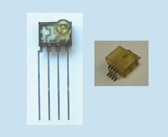
Figure 4. Lead-frame packages for bitcom applications: through hole (left) and surface mount (right).
The outer dimensions of 9.7 mm × 6.2 mm × 3.6 mm are small compared with datacom modules. The FOT contains four electrical leads for through-hole mounting. Two are for power supply, one for data input, and one for control purposes. A barrel feature is integrated in the module housing to facilitate an easy and robust coupling to the ferrule of the external optical cable. The operating temperature of this module is –40 °C to +105 °C for automotive applications and 0 °C to 70 °C for most other applications.
The assembly process includes die attachment of the optoelectronic chips and mounting of the electronics IC chips and passive components onto the lead frame. The optical fiber is aligned to the optical components using a barrel feature in the top part of the package. The top part of the package also contains an integrated optical lens for improved fiber coupling over a wide alignment tolerance range. This is crucial for the usage of very low cost plastic molded ferrules for the fiber coupling.
Conclusion
The key is to design the packaging technology according to the requirements of the application. For the highest performance systems, single-mode optical fibers are used and require high precision and mechanical stability of the packaging system. Therefore metal packages and welding and soldering processes are mainly employed. Butterfly packages are most common in telecom applications. For datacom, TO-cans are mostly used.
Multimode fibers for intermediate range distances in datacom applications relax the alignment tolerances and thereby can reduce cost. The standard transmitter is based on a TO-can with a VCSEL light source inside. Bitcom components are based on low-cost lead-frame packages. They are nonhermetic and offer wide alignment tolerances. Due to their low-cost structure, they can move the application of photonics into the very short distance range and directly compete with electrical solutions based on copper wire cables.