DAEJON, South Korea, March 18, 2021 — Researchers from Korea Advanced Institute of Science and Technology (KAIST), with domestic and international collaborators, demonstrated direct near-field optical imaging of acoustic graphene plasmon (AGP) fields, using a sensitive scattering-type scanning near-field optical microscope (s-SNOM) to directly measure the optical fields of the AGP waves propagating in a nanometer-thin waveguide. The method enabled the scientists to visualize thousandfold compression of mid-infrared light.
The strategy, they said, paves the way for potential breakthroughs in the practical application of acoustic graphene plasmon platforms for next-generation, high-performance, graphene-based optoelectronic devices with enhanced light-matter interactions and lower propagation loss.
Graphene plasmons are collective oscillations of free electrons in graphene that are coupled to electromagnetic waves of light. The oscillations can trap and compress optical waves inside a very thin dielectric layer separating graphene from a metallic sheet, in a system in which graphene’s conduction electrons are “reflected” in the metal so that when the lightwaves “push” the electrons in graphene, their image charges in metal also oscillate. The phenomenon is known as AGP.
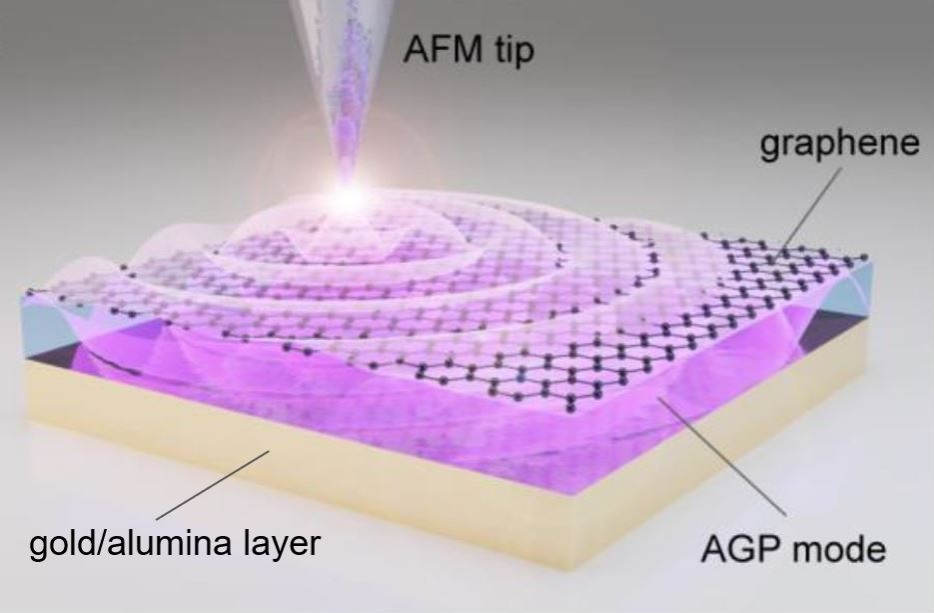
Laser-illuminated nano-tip excites the acoustic graphene plasmon in the layer between the graphene and the gold/alumina. Courtesy of Min Seok Jang, KAIST.
Previously, AGP could only be observed through indirect methods such as far-field infrared spectroscopy and photocurrent mapping; it was believed that the intensity of electromagnetic fields outside the device was insufficient for direct near-field optical imaging.

The new method takes advantage of the decaying, yet always present, electric field above graphene. It showed that AGPs are detectable even when most of their energy is flowing inside the dielectric layer below the graphene. This is due to the presence of ultrasmooth surfaces inside the nanowaveguides, where plasmonic waves propagate at longer distances.
Sang-Hyun Oh, a professor at the University of Minnesota, and In-Ho Lee, a postdoctoral researcher, created the ultrasmooth nanostructures using a template-stripping method. Young Hee Lee and his team at the Center for Integrated Nanostructure Physics of the Institute of Basic Science at Sungkyunkwan University synthesized the graphene with a monocrystalline structure.
The work holds implications for the improvement of chemical sensing detection, as properties of organic molecules can be detected and evaluated based on their absorption signatures in the mid-infrared spectrum. However, conventional detection methods need a high number of molecules to function at optimal levels. The ultracompressed AGP fields can provide strong light-matter interactions at the microscopic level, and improve detection sensitivity down to a single molecule.
The study, led by KAIST professor Min Seok Jang and his team, further demonstrated that the mid-infrared AGPs are less sensitive to losses in graphene due to their fields being mostly confined within the dielectric. The results suggest AGPs as a potential platform for electrically tunable graphene-based optoelectronic devices — which typically suffer from higher absorption rates in graphene — such as metasurfaces, optical switches, photovoltaics, and other optoelectronic applications operating at infrared frequencies.
The research was published in Nature Communications (www.doi.org/10.1038/s41467-021-21193-5).