It is almost a cliché among students of creativity that innovation occurs at the intersection of fields. Since nanopositioning is a discipline that has enabled swiftly evolving application arenas as diverse as materials science, genomics, photonics, defense, biophysics, and semiconductors, it’s unsurprising that its pace of innovation is nothing short of blistering in recent years.
Scott Jordan, Brian Lula, and Stefan Vorndran, PI (Physik Instrumente) LP
By its original definition, a nanopositioning device is a mechanism capable of repeatedly delivering motion in increments as small as one nanometer. Lately demands from industry and research have driven requirements to 1/10th nanometer and below.
While electroceramics such as piezo materials with flexure guides remain the gold standard for breaking the resolution nanometer barrier, there are several other commercial solutions available today providing repeatable single-digit nanometer step resolution including linear motors, voice-coil drives, and frictionless guides such as air bearings and magnetic bearings.
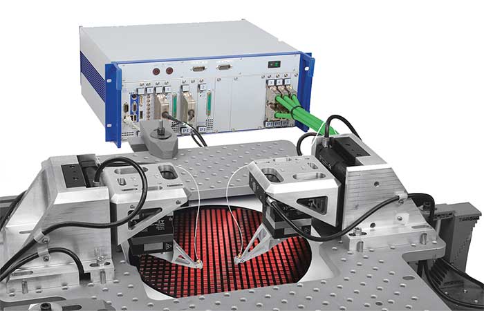
Figure 1. A test and alignment system for silicon photonics wafers based on closed-loop motorized XYZ micropositioning stages and piezo nanopositioning stages to combine the fastest alignment speeds with the highest flexibility.
The recent innovation poses both benefits and challenges for engineers and researchers who need to integrate nanopositioning into their applications. Benefits range from enhanced throughput, precision and accuracy to outright enablement of applications that were formerly impossible. But a big challenge is simply keeping up with the latest breakthroughs as they become commercially available, and leveraging the best of them without accepting unnecessary technical risk.
Choosing the right nanopositioning system means, ideally, that the vendor understands the complete application, ranging from specifications for resolution, accuracy, travel and throughput to the development environment, interfacing, and synchronization needs.
Of course, cost metrics — which include not only purchase price but cost-of-ownership — are critical for all parties to understand. Deeply functional, well-documented and robust software-support libraries that facilitate rapid application development are increasingly important for accessing advanced functionalities, reducing support costs, and compressing time to market in today’s multi-platform world. Custom solutions are often required, and the vendor’s wherewithal, technical depth, global support capabilities, adherence to international quality standards, and organizational stability are key to successful long-term partnerships. Cognizance of today’s stringent export control regulations is also important for many customers.
More and more, dynamic issues dominate applications, with novel approaches that benefit real-time/high-dynamic applications. These present new opportunities for optimizing process economics.
In fact, optimization is often the application in a nutshell, for example in the rapid fab-floor testing and packaging of today’s new generation of silicon photonics (SiP) devices. In these applications, optical elements and probes must be rapidly brought into perfect coupling with devices in various stages of manufacture from wafer to final package. Here, simple economics necessitates that nanoscale mutual alignment be achieved in a second or less. The novel solutions that have emerged to enable these applications are position optimization engines, representing a new class of positioning system that relies on the device-under-test for position information as much as it does its own encoders.
Fab-class applications have considerations of their own. If, for instance, you are optically probing a fully patterned SiP wafer worth millions of dollars, the ability of the positioning system to be programmatically limitable is critical for wafer safety. This demands an all-digital controls approach, since analog alternatives (though cheaper) are difficult to constrain reliably. Similarly, cleanliness, cable lengths, EMI, and other attributes can factor into a specification.
Long travel friction-free nanopositioning systems
As a rule of thumb, the lower the mechanical friction in a motion system, the higher the positioning performance at the nanometer level is to be expected. Guidance remains a concern: stiction effects limit the effective minimum incremental motion of even the best mechanical bearing systems in long-travel stages. Three frictionless guiding systems are often used in nanopositioning applications: flexures, air bearings, and magnetic bearings. Piezo nanopositioning systems are often guided by flexures, which are stictionless yet highly stable and stiff, but with travels limited to the millimeter region and below. For longer travel ranges air bearings are also very successful in precision industrial motion applications. An air-bearing stage is a linear or rotary positioner that floats on a cushion of air, using one of several preloaded mechanisms, virtually eliminating mechanical contact and thus wear, friction, vibration, and hysteresis effects.
A slotless direct-drive motor with the help of a high-resolution optical encoder or interferometer can position a moving carriage supported by an air bearing to within nanometers in a linear application, or within 10ths of arc-seconds in rotational applications. The lack of friction and mechanical contact means there is minimal hysteresis or reversal error, making it highly repeatable and ideal for many inspection and manufacturing operations. Stiction is virtually eliminated, improving resolution capabilities and reducing in-position “hunting” (limit cycling), and position repeatability can be obtained within a few fundamental encoder counts. Air bearings can also be locked down to provide extremely good in-position stability and long term stability.
Due to the surface averaging effect, air bearing stages can claim not only very low overall straightness and flatness error motions, but also extremely repeatable and stable errors as well.
Air-bearing nanopositioning stages are used in high precision motion applications, such as metrology, semiconductor, flat panel display inspection, and other precision scanning applications. The noncontact design also makes these stages work well in cleanroom applications.
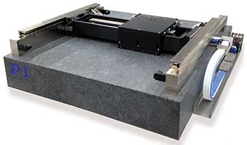
Figure 2. A three-motor planar XY air-bearing nanopositioning stage with active yaw control via a highly engineered flexural coupling that provides yaw-compliance without sacrificing system stiffness.
Active magnetic bearings/magnetic levitation
Magnetic bearings replace mechanical contact with electromagnetic fields. When combined with magnetic levitation, multi-axis planar positioning stages can be designed with a passive platform levitated by a computer controlled magnetic field which also guides the platform actively. Objects can be positioned linearly or rotationally over long travel ranges with exceptional guiding accuracy. Magnetic levitation positioners can achieve similar performance to air bearing positioning stages. As there is no friction, there is no wear which could contaminate the work space. Furthermore, neither air nor grease are needed for lubrication, making magnetic-field-based systems perfectly suitable for applications in vacuum or nitrogen atmosphere.
Short travel nanopositioning stages/piezo positioners
Flexure guides provide many advantages for short travel applications in the millimeter range and below. Just like air bearings and magnetic bearings, they are frictionless. However, they can be made extremely small and robust, at lower cost. Flexures are often combined with a number of frictionless drive systems from voice-coils, to linear motors and solid-state actuators.
Flexure guides are also employed in the vast majority of piezo-driven nanopositioning systems.
Piezoelectric technologies play a foundational role in positioning applications with nanometer resolution and below requirements. The direct piezo effect was discovered more than 100 years ago and today’s nanopositioning devices capitalize on the inverse effect, using a voltage to provide motion via material expansion. Most such devices use a polarized ferroelectric ceramic material made from lead, zirconium, and titanium. Consequently, they are often called piezoelectric transducers, or PZTs — an acronym which reflects their chemical constituents. (see sidebar below.)
The benefits of piezo-based devices include:
• Unlimited resolution: Positioning increments well below 1 nm are possible. This is critically important for applications ranging from semiconductor lithography to superresolution microscopy and optical tweezers. However, precision performance requires carefully designed and manufactured mechanisms; otherwise incremental motion can be limited by stick-slip effects, mechanical losses, parasitic motion errors, and suboptimal metrology implementation.
• Fast expansion and response (microsecond time constants).
• Maintenance-free, solid-state construction that reduces wear and eliminates scheduled maintenance, lubrication, or adjustment even with heavy usage.
• High efficiency: Electrically, piezoelectric elements resemble capacitors, in that energy is absorbed only to perform movement, not to maintain position.
• Inherent vacuum-compatibility (especially for the newest ceramic-encapsulated piezo stacks).
• Non-magnetic and magnetic-insensitive construction. Being ceramic devices, piezoelectric elements are impervious to magnetic fields and produce none of their own. When paired with appropriate structural materials and bearings, virtually fieldless and field-insensitive mechanisms can be constructed.
• High throughput and dynamic accuracy, especially when newer controls technologies are leveraged.
• Finally, piezoelectric technology has been applied in novel mechanisms that provide many millimeters of travel while maintaining better than nanometer resolution.
Industrial reliability
Most piezo ceramic actuators are constructed of many layers sandwiched between electrodes, similar to ceramic capacitors and traditionally made using polymer coatings on the outside as insulation. But polymer coatings also trap moisture, leading to limited lifetime. Then, with the advent of high-duty-cycle, high-dynamic, uptime-critical industrial applications, traditional encapsulation began proving inadequate to protect sensitive mechanisms. High-dynamic industrial applications often resulted in heating which could be problematic for polymer coatings, and nanopositioning was increasingly important in vacuum applications such as e-beam lithography and microscopy.
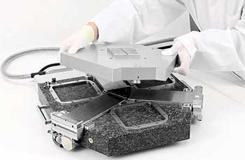
Figure 3. A six-axis positioning stage based on Hallbach array linear motors, active magnetic bearings, and magnetic levitation.
Consequently, all-ceramic-encapsulated, cofired piezo actuators were introduced pushing performance and reliability to new limits. The novel use of cofired ceramic encapsulation makes these actuators several orders of magnitude more impervious to humidity, greatly improving the reliability of devices based on them, especially when used in challenging environments. Materials that extend the temperature range to 150 °C allows them to be run in hotter environments, baked for high-vacuum compatibility, or driven harder and faster in dynamic operation. In fact, NASA/JPL engineers ran these actuators through harsh life tests including 100 billion expansion/contraction cycles before selecting them for the Mars Rover’s science lab.
Long-travel piezo technologies
So far our discussion has centered on stacked piezo actuators where the layers all actuate longitudinally when a voltage is applied, lengthening the stack and providing positioning control well below 1 nm. But layers can also be configured to actuate in shear mode, conferring in-plane motion.
By combining lateral actuation and longitudinal actuation, the basic element of another significant class of new mechanisms, PiezoWalk, is constructed. In this family of motion devices, groups of piezo elements are preloaded in arrays about a central rod. A digital controller sequences their operation, providing high-force, long travel step-mode actuation plus picometer resolution fine high-bandwidth actuation. Several motion-device families are now available within this general class of technology. All are inherently vacuum-compatible and fieldless, and they provide nanoscale power-off position stability for months and years. Standard designs provide forces to 800 N, resolution to 50 pm and travel to many millimeters. This combination of high force, high resolution, stability, and long travel is proving to be an enabling technology for a wide variety of microlithographic, nanoimprint, and astronomy applications requiring high force, high stiffness, high stability, and picometer resolution over millimeters of travel.
Another use of piezo ceramics technology is in ultrasonic piezo motors. These are not stacked structures but instead are composed of monolithic slabs of piezo ceramic that are used to drive standing waves in the substrate at frequencies of tens to hundreds of kilohertz. A hardened contact-point, or finger, attached at a resonant node-point is thereby made to oscillate in a quasi-elliptical fashion; when preloaded against a slide, this confers linear motion. These piezomotor implementations achieve up to 500 mm/sec velocity over virtually unlimited travel ranges while providing nanometer precision and high fast start/stop dynamics. A key benefit of this class of motor (when implemented properly) is their in-position stability. Since the nanoscale lubricant flow that occurs within screw-driven mechanisms is eliminated, the stability has been demonstrated to be significantly better than that which can be achieved with conventional mechanisms in leading-edge microscopy applications.
Yet another piezo-technology innovation is found in miniaturized mechanism based on the inertia motor (stick-slip) effect. Stick-slip piezo motors provide lower speed compared to ultrasonic motors, but are extremely compact and cost-effective. These tiny stages are the size of a thumbnail, yet provide many millimeters of travel with closed-loop operation and linear encoders featuring 1 nm resolution.
Nanopositioning goes hybrid
New controller technologies have made it possible to devise hybrid nanopositioning systems employing both PZTs or voice-coils and servomotor drives. These systems combine the properties of unlimited resolution and very fast response with the long travel ranges and high holding forces of a servomotor/ballscrew arrangement. A highly specialized hybrid controller reads the stage position from an integrated, nanometer-class linear encoder and continuously coordinates both the piezoelectric (or voice coil) short-travel and servomotor long-travel drives in a way to provide the best possible overall performance, with rapid pull-in, nanometer-scale bidirectional repeatability and inherent axial stiffness that are unobtainable from conventional architectures. The result is a fast, long-travel system with extraordinary repeatability as well as resolution.
Sensors/controllers for closed loop operation
Achieving nanometer and subnanometer precision requires more than a piezo actuated stage capable of making moves on this precision scale. The stage internal metrology system must also be capable of measuring motion on the nanometer scale. The primary characteristics to consider when selecting a stage metrology system are linearity, sensitivity (resolution), stability, bandwidth, and cost. Other factors include the ability to measure the moving platform directly and contact vs. noncontact measurement.
Three types of sensors are mostly used in nanopositioning applications — linear encoders (for longer travels), and capacitive and strain sensors (short travels).
Linear encoders are familiar devices for measuring long displacements up to hundreds of millimeters and the best units now reach below the single digit nanometer resolution realm. Traditional linear encoders use optical or magnetic scales and readhead elements. Optical units function by observing the first-order diffraction between a scale composed of finely pitched lines or facets and a similar moving reticle. By nanopositioning standards, the period of the scale is often fairly gross, typically several to several dozen microns for moiré scale or holographic encoders. Position is determined by counting fringe transitions and by interpolating between adjacent peaks — resolution is increased by up to 10,000 times or more. While resolution in the subnanometer range is common, accuracy is typically limited to 1 micron per 100 mm. However, this can be improved significantly with modern controllers calibrated and compensated for with look up tables or polynomial error correction.
While incremental linear encoders provide higher possible resolution, their coordinate system must be re-established at each initialization by seeking a reference signal, a procedure that can be time consuming and accuracy limiting. Absolute position encoders don’t require referencing and are catching up in terms of resolution and affordability.
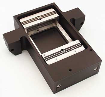
Figure 4. Flexure-guided, voice-coil, motor-driven positioning and scanning stage.
For short travel nanopositioning devices, cost-effective strain gauges (including piezoresistive sensors) use elements whose electrical characteristics change with strain. These devices are usually attached to the piezo ceramics itself, or possibly to a structural element of the positioning stage. Consequently, they serve as drivetrain-input metrology rather than independent, direct motion metrology of the moving platform of the stage. Nevertheless, these are popular and effective position-metrology elements in closed-loop systems. They can provide high sensitivity, are compact, and are adequate for positioning to subnanometer resolution levels. They provide absolute position measurement, require no initialization, and can be acceptably stable if good signal conditioning approaches are implemented. Good implementations incorporate multiple sensors and bridge circuits to compensate for thermal changes. But care must be taken when designing them into a mechanism. If there are elastic or frictional elements in the path between the point of motion and the point of measurement, errors will result. Physically small sensors (such as piezoresistive sensors) measure only a highly localized region’s strain, from which the overall mechanism’s motion must be inferred. And these sensors cannot be configured to compensate for orthogonal (parasitic) errors in multiaxis configurations — only parallel metrology of the actual moving platform can provide this valuable capability.
Interferometry also can be used to measure sample position and provide a feedback control signal. Such systems offer extremely high accuracy and are noncontact, although bulky specialized optics must be mounted onto the moving and stationary elements of the motion system, and safety provisions for beam blockages and eye safety must be considered. Interferometers can be deployed in vacuum systems by feeding laser light through a window or fiber. Some interferometers can provide subnanometer resolution, though cyclic inaccuracy can be noted in some units.
Because interferometers use air as their working fluid, they can be sensitive to environmental factors (temperature, barometric pressure, humidity, trace gas concentration, and acoustic perturbations). Interferometry tends to be costly, and drift can be problematic, particularly for lower-cost units. Available interferometers are also relative position devices that must be initialized at a repeatable zero position determined by some other metrology incorporated into the motion system.
Capacitive sensors have emerged as the default choice for the most demanding nanopositioning applications requiring short travel ranges. They are extremely accurate, ultrahigh-resolution devices for determining absolute position over ranges of hundreds of microns or even millimeters. The device’s positioning motions vary the distance between two nano-machined capacitor plates, providing a sensitive and drift-free positional feedback signal when stimulated by a precision AC carrier. No “home switch” is needed, so day-to-day repeatability is superb.
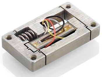
Figure 5. A motion amplified, flexure-guided actuator based on a multilayer piezo stack. Electroceramic drives such as piezo stacks are at the heart of many nanopositioning systems. The latest designs use full-ceramic-encapsulation for longer lifetime and UHV compatibility. Piezo flexure drives can last 100 billion cycles and provide exceptional resolution down to the picometer range with fast response in the microsecond range. Travel ranges are typically below 1 mm.
The best examples of these sensors offer high bandwidth with high precision. They are noncontact and are usually packaged to measure drive-train output (direct metrology) — eliminating errors otherwise imposed by intervening mechanisms. The physical characteristics of capacitive sensors make them ideal for multiaxis parallel kinematics approaches, where a single monolithic moving platform is actuated simultaneously (and measured simultaneously) in several degrees of freedom. This allows active compensation of parasitic errors, which cannot be achieved with stacks of discrete axes. In addition, parallel kinematics facilitates more compact packaging, greater mechanical rigidity, higher throughput and greater dynamic accuracy in real-time applications. Meanwhile the single-frequency stimulation of capacitance sensors is inherently resistant to external noise sources.
Active optic mounts
Piezoelectric devices lend themselves well to linear or tip/tilt mechanisms and multiaxis configurations combining multiple linear and rotary degrees of freedom. In linear stage or actuator application, they can achieve resolutions well below 1 nm, and in rotary and tip/tilt applications, resolutions surpassing 1/100 arcsec.
Compact piezo-actuated active optic mounts are available with multiple degrees of optical deflection. Two-axis, parallel-kinematic piezo mounts offer gimbal-style actuation with coplanar rotational axes, a significant advantage vs. the separate orthogonal mechanisms that are often required of galvanometer-driven approaches that also bring about the drawback of polarization rotation. Compared to galvos and voice-coil systems, piezo-driven active optic mounts are typically more compact, fieldless, faster, inherently stiffer, and more predictable when power is cut. Lower current requirements mean reduced ohmic losses and heat production, and cabling is thinner and more tractable. Piezos’ flat Bodé curve means higher responsiveness through more of their dynamic range than is often possible with alternative drives.
Throughput, speed, and precision: electroceramics
If very rapid movements are needed, piezoelectric devices are often the only solution. Piezoceramic positioning devices can have bandwidths of tens of kilohertz or more, and they lack the responsiveness-limiting inertia of leadscrews and other conventional mechanisms.
Unfortunately, advancing resolution needs in industry and research are physically at cross-purposes to advancing speed needs. In this way, applications’ increasing need-for-speed coupled with unabated pressure on resolution capabilities exposed fundamental physical limitations of traditional nanopositioning technologies, especially for controls:
• Electronic bandwidths, limited by amplifier, sensor, and servo-processing capabilities, cause “rounding of corners” in motion-waveform generation, phase-lags, and nonlinearities in high-dynamic applications.
• Mechanical stiffness, characterized by the lowest resonant frequency (Fres) of the mechanism, limits the accurate controllability of a mechanism in high-dynamic applications.
Traditional approaches to improving matters include using higher power amplifiers, faster servo update rates, stiffer materials, and so on. However, these merely push the margins of system performance back incrementally, and sometimes with a very poor cost/benefit ratio. In addition, applications requiring varying loads often force compromises, such as servo settings which are safe for all intended loads but optimum for none.
Figure 6. An XYZ nanopositioning flexure stage for superresolution microscopy.
There are additional error mechanisms that come into play when nanopositioning mechanisms are actuated rapidly in motion waveforms:
Observable resonance
• Actuation profiles that contain Fourier components near Fres will result in resonant amplification and possible runaway.
System roll-off and servo lag
• Finite electronic bandwidth in the servo controller and amplifier results in roll-off of high frequency components of the desired motion waveform.
• When Fres is on the order of motion waveform components of interest, this can provide additional roll-off behavior on either side of Fres.
• The error-driven nature of feedback-based servos imparts a lag between command input and motion output. Combined with frequency-dependent roll-off, this can distort the motion waveform output, shifting it in time and rounding fine features undesirably.
• Propagation delays in some digital implementations can impart additional lags between command and motion.
Unobservable resonances
• Fres generally refers to the primary resonance of the device, but other resonances can certainly exist in any motion system, especially when external componentry is considered, such as the stage’s load, mounting structure, and neighboring components — all of which can be driven to ringing by recoil forces in rapid actuation.
Optimizing the mechanics
Obviously, the stiffer the mechanics, the crisper their responsiveness to motion commands: Fres rises, and roll-off is pushed to the right in the system’s Bodé plot, improving dynamic accuracy.
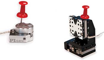
Figure 7. Miniature piezo inertia motor-driven nanopositioning stages. Rotary stage with 14 mm diameter (left) and XZ combination, 22 mm travel, 1 nm resolution (right).
A highly effective technique for raising Fres while simultaneously addressing parasitic motions in multiaxis systems is to “attack the stack,” replacing the traditional design approach of using bolted together or nested layers of single-axis mechanisms with a single moving element actuated and monitored by parallel arrays of actuators and sensors. This approach, parallel kinematics, reduces the actuated mass while improving stiffness. Thus both parameters in the Hookes equation for resonance are optimized. A key advantage is seen in the improved runout performance when any given axis is actuated: the other axes will actively cancel unwanted parasitic motions, resulting in truer trajectories and automatic compensation for loads and external forces which might otherwise deflect the mechanism. Parallel-kinematic stages providing two to six degrees of freedom are offered. Systems offering four or more degrees of freedom usually feature digital controllers which automatically perform coordinate-system transformations so the user can work with familiar units and Cartesian conventions.
There are a host of other considerations in the motion device design which can impact stiffness. For example, travel and form factor requirements may necessitate lever amplification. Lever amplifiers influence stiffness in motion direction of a nanopositioner; stiffness coefficient diminishes with the square of the lever amplification ratio. The effective stiffness of the mechanism is also impacted by mounting considerations by the user. For the load, the moment arm of the center of mass with respect to the symmetry axis of the motion device’s platform should be kept as short as possible. In rapid actuation, CG offsets above or to the side of the symmetry axis can excite pitch and yaw moments, respectively; dynamic accuracy can actually be improved by counterbalancing in these situations, even if this means adding mass. And certainly the mounting hardware should be as rigid as possible; stiffnesses “add” as a sum of quotients.
Optimizing the controls
Conventionally, the various roll-off and lags presented by servo controls, amplifiers, and feedback mechanisms can be incrementally improved by selecting higher-power amplifiers, faster servo update rates, and so on. However, these efforts pay diminishing returns and fail to address the root-cause physics of dynamic inaccuracies. Fortunately, recent technical developments present a selection of tools which can improve matters.
Downloadable servo parameters: Digital controllers allow virtually instant download of servo parameters for different loads, rather than forcing the user to deploy a lowest-common-denominator parameter set for safe (but suboptimal) operation with all anticipated loads.
Notch filters: Resonant amplification at Fres (and roll-off to either side of it, as is often seen) can be addressed via a notch filter in the controller. Amazingly, not all piezo controllers have notch filters, necessitating softer servo settings to eliminate the risk of oscillation and runaway. Softer settings mean poorer dynamic accuracy.
Simple feedforward: This technique, popular with motor controllers, involves injecting a portion of the command signal directly to the amplifier, bypassing the servo. Since piezo devices operate in the 0th derivative of position, this technique is more problematic than is the case with servomotors, which operate in the 1st derivative. Dynamic accuracy can be reduced in simplistic implementations.
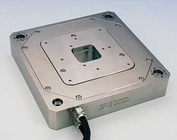
Figure 8. A six-axis nanopositioning stage with active trajectory control, made from super invar. These types of stages can provide subnanometer resolution and straightness/flatness of travel in the subnanometer range and are often used in AFM applications.
Digital dynamic linearization (DDL): This control technique integrates an internal algorithm into the metrology and servo logic; this optimizes the internal command generated for a repetitive waveform according to the error signal that is detected with the internal sensor. It is the latest advancement for improving dynamic accuracy. It was originally deployed in a precision automotive machining application in the 1990s, as a patented off-line technology called Signal Preshaping, where it provided the bandwidth enhancement necessary to machine advanced noncylindrical pistons at economically acceptable lathe spin speeds. A fully automatic, fully internalized implementation, DDL shipped in 2002. A brief, automatic self-configuration is commanded by the user (or, previously saved optimizations may be reloaded) when changes in motion parameters, desired waveform, or loading occur. After this, following errors are reduced to approximately the noise level of the system.
Input shaping: In many applications, fast actuation of the nanopositioning stage causes its load and neighboring components to ring with their characteristic resonant frequencies. These oscillations may not be observable by the motion feedback sensor, so finessing servo parameters is of limited utility. Input shaping is a patented time-domain feedforward technique which nullifies these unobservable, motion-driven resonances to improve system dynamic accuracy. The systems integrator first quantifies the frequency of the vibrations (often this falls out of the system’s work product); the controller is then informed of these by downloading a real-time parameter set into nonvolatile RAM. From that point on, no commanded motion will excite the resonances. The technique accommodates multiple resonances, nonorthogonal resonances which trade energy between themselves, and any degree of damping.
Energy recovery: An amplifier was developed for high-force/high-dynamic applications utilizing piezo actuators of large capacitance. This amplifier design integrates unique energy-recovery technology and pulse width modulation. Instead of dissipating the reactive power in the heat sinks, charge is recovered so that only the active power used by the piezo actuator has to be supplied. During discharge of the actuator, the energy not used is returned and reused to supply the amplifier. Production versions of this amplifier can output and sink a peak power of 2 kW.
DAC resolution enhancement: Piezo expansion is approximately proportional to the applied voltage. Consequently the smallest motion that can be commanded is approximately proportional to the smallest voltage increment that can be applied. Almost universally, the voltage is ultimately commanded by a digital-to-analog converter (DAC). These can reside in the piezo controller or in the customer’s PC. In the latter case, very flexible and sophisticated software programming environments exist for generating waveforms and synchronizing with other processes and instrumentation. Sophisticated digital piezo controllers offer similar functionality, but the flexibility of PC-based analog I/O makes it very popular.
True to their name, DACs take a digital number as their input and produce a voltage in response. Their voltage resolution — their granularity — is equal to their voltage range divided by 2N, where N is the bitwidth of their digital command. A 12-bit DAC can therefore split the DAC’s voltage range (e.g., 0 to 10 V or -10 to +10 V) into 4096 distinct values. A 16-bit DAC can divide its voltage range into 65,536 steps.
The most popular instrumentation grade analog I/O cards for PCs top out at 16 bits. However, economic and application prerogatives increasingly necessitate longer and longer travel piezo mechanisms. Precisely guided stages with up to 1800 µm travel are now available for these applications. A customer limited to a 16-bit DAC would achieve only about 28 nm resolution from such a stage due to DAC granularity. In many applications that would not be good enough.
A patented technology, HyperBit, takes advantage of the fact that as fast as piezos are, DACs are often faster. By performing high-speed modulation of the DAC at a rate at which the piezo system cannot respond to, up to 11 additional bits of resolution positioning can be achieved with no loss in positioning bandwidth or stability. Both waveform and quasi-static positioning, open- or closed-loop, can benefit. The technology preserves legacy investments in software and analog I/O hardware.
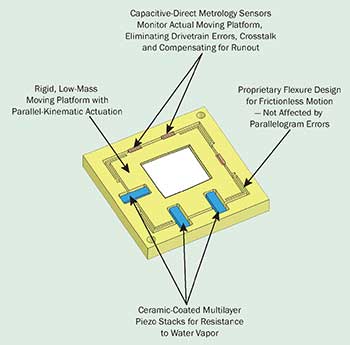
Figure 9. Piezo flexure nanopositioning stages with capacitive sensors for high resolution, bandwidth, and stability enable applications such as nanometrology or optical trapping. Parallel-kinematics/parallel-metrology designs offer superior motion fidelity by positioning and measuring a single platform using multiple actuators and sensors against the same stationary reference.
Interfacing
A wide variety of instrumentation interfaces is available in today’s marketplace, ranging from the venerable and robust RS-232 to Ethernet, SPI, and USB, plus a host of specialty interfaces. All have advantages and disadvantages and since nanopositioning and motion controllers communicate via short messages, latency is often much more important to overall throughput than bulk transfer speed. USB and Ethernet are ubiquitous and easy to use, with the latter supporting remote and distributed communications at the cost of variable latencies.
Intriguingly, although analog interfacing is the oldest of all, it has essentially zero latency and infinite speed and is easily coordinated with data acquisition, triggering and other real-time processes. However, until recently, programming an analog application was left as an exercise for the user, with the controller manufacturers’ LabVIEW and other software libraries devoted to the various digital interfaces. A recent innovation was the introduction of analog-interface support by one manufacturer which includes LabVIEW subroutines (sub VIs) that perform point-to-point and waveform positioning out of the box, within a consistent software architecture that transparently supports multiple controller models and all available interfaces. This greatly facilitates rapid application development and code re-use, while allowing compatibility with alternative controllers.
One thing to keep in mind when discussing your application with a nanopositioning supplier is that there is much more to a digital controller than a digital communications interface. Adding a communications port and an internal DAC to an analog servocontroller might limit you to point-to-point applications of modest throughput. Better implementations add internal waveform generation and synchronization capabilities; the highest-performance implementations are of course fully fledged DSP architectures which eliminate the analog servo circuitry entirely. These are the truly digital controllers.
Formats and applications
Applications such as atomic force microscopy (AFM), the alignment of photonic assemblies, surface profiling, photolithography positioning, wafer/mask inspection and repair systems, and optical tweezers already use piezoelectric devices. Near-field probing, scanning-probe microscopy, and disk-drive test applications are using a new generation of piezoelectric technology that provides subnanometer and subarc-second precision. These systems employ actively or passively compensated trajectory control for nanometer-scale flatness, straightness and planarity, and allow bidirectional processing for throughput.
Systems are available that — besides applying closed-loop principles to single-axis nanopositioning mechanisms — integrate an XY nanopositioning stage with six-axis active trajectory control. Active trajectory control requires a parallel kinematics design with noncontact sensors in a parallel metrology configuration. At PI, we have developed one that provides
200 × 200 µm XY motion with compensation for unwanted out-of-plane Z and rotational motions.
Digital control systems offer advantages over analog control systems: real-time linearity compensation, elimination of some drift mechanisms (with high-resolution DAC residing inside the servo loop), advanced interfaces, waveform-generation capability, and other features that only a digital architecture can provide. But some digital implementations lack the functionality of a well-designed analog implementation such as high bandwidth, fast settling time, compatibility with advanced feed-forward techniques, stability, and robust operation. Engineers would be wise to weigh the advantages of seemingly leading-edge implementations against characteristics such as responsiveness, stability, cost, noise immunity, resolution, and the ease of use of proven designs. A vendor’s design philosophy can also have profound impact on overall system performance; for example, unsophisticated designs can rely on a comparatively low bit-width DAC inside the servo loop, driving a low-bandwidth amplifier which allows the DAC to meander between adjacent bits, providing resolution at significant cost to short-term stability and throughput.
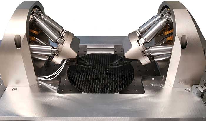
Figure 10. Hexapod parallel-kinematic positioners provide 6° of freedom and a programmable pivot point. Units with load ranges up to 5 tons and sub-micrometer precision are available today. Shown here is a dual 6-axis miniature hexapod nanopositioning system combination with high-speed XYZ piezo flexure scanners for millisecond range tracking and alignment applications.
Another advantage is the integration of a calibration chip into motion devices. This allows the controller to download device-specific parameter and calibration information. Although convenient for repair situations, it is no substitute for a robust and reliable design that avoids repair issues in the first place.
Some recently developed technologies have potential application to both analog and digital control implementations.
A particularly common application of nanopositioners to photonics is in automated alignment. This is a fundamental step in virtually all of today’s photonic device-packaging operations, and the speed and reliability of the methodology and devices selected drives the yield and overall economics of the manufacturing operation.
The first automated alignment systems were laboratory-grade instruments that were introduced in the late 1980s. These utilized a piezo dithering mechanism and an analog phase-demodulation scheme which drove a high-resolution alignment stage. Several of these systems are still offered.
The analog phase-demodulation technique is one of several types of “gradient search” methods. Gradient searches are suitable for rapid alignment of clean, unimodal, quasi-Gaussian coupling cross sections, and in these cases their alignment can be very rapid, concluding in a few seconds and tracking drifts from there on. However, this method has a habit of locking-on to the first “flat spot” they encounter in the coupling. Hence, they are inappropriate for many (perhaps most) real-world packaging applications. Brute force raster and spiral scan techniques can be effective in some applications and are the foundation for many heavier-duty systems that have been implemented by device manufacturing engineers and their systems integrators. These are generally based on stacks of mechanical stages from one catalog or another.
Hexapod 6-D systems
Integrated, industrial microrobots have been introduced to address the general case of industrial photonics packaging automation. The most intriguing of these are based on a hexapod design rather than a stack of stages. This approach allows tip/tilt alignments to be automated in a very flexible fashion since the hexapod approach lets the rotational pivot point be placed anywhere in space via an internal coordinate transformation in the controller. Rotations can thus be centered on a fiber endface, laser beam waist, lens focal point, array axis, MEMS channel, or any other optically desirable place, regardless of fixturing or device variations. This greatly improves the process by addressing parasitic transverse motions that are otherwise unavoidable.
In a fashion, the introduction of these microrobots repeats a script seen in the semiconductor industry two-and-a-half decades ago. Back then, manufacturing yield issues drove the elimination of manual wafer handling.
The first handlers were straightforward stacks of linear shuttles that bore more than a passing resemblance to the stack-of-stages approach to fiber alignment. Eventually a multilink, coaxially rotating format was introduced. At first dismissed by some as outlandish or needlessly complex, this type of handler quickly gained acceptance thanks to its inherent throughput, cleanliness, and real-estate advantages. Similarly — although the field of photonics alignment microrobots is very new — the rapid acceptance of hexapod-format microrobots, thanks to their inherent alignment and format advantages, may represent a new manufacturing standard emerging before our eyes.
Circling back
A recurring theme is that choosing a vendor represents a choice of partner, and this brings us back to our opening theme. Beyond the fundamentals of product capability, quality, global support, and applications savvy, there’s the benefit of working with a supplier whose experience crosses many fields and many drive technologies. Such a supplier is in a position to offer insights and best-practices from other arenas. This sort of cross-pollination can help you drive innovation in your application, keeping you a step ahead.
How Piezo Actuators Work
Physically, a linear piezo actuator consists of a series of stacked cylindrical PZT ceramic elements. The cross section is usually either square or circular. Each disc has metal contacts for the application of a voltage parallel to the direction of polarization. The ceramic is formulated to present an electrostatic dipole moment on the molecular scale. The applied electric field exerts torque on the dipoles, causing a change in the length of the monocrystalline regions. This causes the stack to expand and contract (or shear) in approximate proportion to the applied voltage, allowing control of position to subatomic precisions.
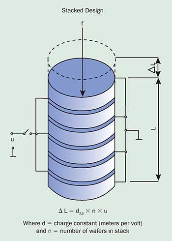 Most piezo actuators are designed to provide motion ranges of 5 to 300 μm. This range is determined by the composition, length of the material, maximum applied voltage and other factors. Typical PZTs feature a 0.13 percent strain, meaning a 100-mm-long stack can expand to 130 μm when the maximum allowable voltage is applied.
The basic piezo actuator stack is the heart of the nanopositioning stage. High-precision, stiction-free flexure lever amplification and guidance mechanisms allow stage travels to 1 mm. Stiction, looseness, rigidities and guidance quality all factor heavily in the device’s overall performance and require meticulous and highly specialized design and manufacturing skills. For reproducible nanometer-scale accuracy and reliability in industrial-class applications, extraordinary mechanical quality must be maintained throughout the mechanism.
However, stage design and construction quality can vary greatly, particularly in multiaxis designs where traditional stacking and nesting techniques can compromise performance and throughput. Caution dictates a close collaboration between engineer and vendor to evaluate all aspects of performance, such as out-of-plane motion, step/settle response, and EMI immunity, rather than just relying on nominal specifications.
Linear piezo actuators are typically built from thin, stacked PZT layers.