Higher power, denser pulse repetition frequencies, and shorter wavelengths are introducing new opportunities in diverse markets.
Chandra Nathala, Jim Bovatsek, and Herman Chui, MKS Instruments
Commercial use of ultrashort-pulse lasers, and femtosecond pulsed lasers in particular,
continues to rise, due to the ability of these sources to cleanly ablate material or tissue with minimal heating of and damage to surrounding areas, and with negligible debris generation. Today, femtosecond lasers find use in a wide range of applications, including eye surgery, fabrication of implantable medical devices, photovoltaics scribing, surface functionalization, glass cutting, and polymer film cutting for the manufacture of displays and microelectronics. In micromachining applications, there is an especially strong demand for higher power and repetition rates to achieve the higher throughputs necessary for high-volume manufacturing. Femtosecond lasers operating in the ultraviolet (UV) are also increasingly needed to process more heat-sensitive materials or to achieve extremely high-quality results.
Increasingly capable laser technology
Keeping abreast with these demands, laser manufacturers continue to scale up femtosecond laser power levels and pulse repetition frequencies, while offering shorter wavelengths. In the past two decades, the average power of commercial infrared (IR) wavelength femtosecond lasers has increased by roughly two orders of magnitude. More recently, industrial femtosecond lasers offering green or UV wavelengths, excellent beam quality, superb pulse-to-pulse stability, and higher power levels have also emerged on the market (Figure 1).
Figure 1. An industrial UV femtosecond laser with >50-W output power. Courtesy of MKS Instruments.
The advent of high-power, high-repetition-rate femtosecond lasers does not by itself lead to high-throughput processing. It is well known that an optimal fluence (energy density, typically in J/cm2) exists for efficient ablation that thereby reduces thermal damage to the surrounding material. This optimal fluence has been shown to be approximately e2 (or ~7.4) times the threshold fluence1. The practical implications of this are that high-energy pulses become efficient only by increasing the spot size (and correspondingly the scan speed), by increasing the number of spots for parallel processing (via beamsplitting), or by splitting pulses into many subpulses of lower energy (burst pulses).
The first two approaches require costly, very high-speed scanning equipment or additional optics for beamsplitting. Industrial femtosecond lasers capable of generating burst pulses are now offering a viable alternative. In burst-mode operation, a single high-energy pulse is split into several lower-energy pulses to essentially achieve a more optimal fluence by tailoring optical output in the temporal domain. In some advanced implementations of this technology, the burst envelope can be shaped — that is, the energy of each subpulse in a burst can be varied.
Figure 2 (top) shows burst pulses from a 100-W IR femtosecond laser, in which the energy of a 9-pulse burst is shaped to fit within three distinct energy regimes, with an ~5× total range in energies. Figure 2 (bottom) shows the volume ablation rates in stainless steel as a function of power at a 1-MHz repetition frequency and with all burst pulses having equal energy. The optimal ablation rates are obtained at high average powers by increasing the number of pulses in a burst. The approach leads to a fewfold enhancement of material removal rates in stainless steel.
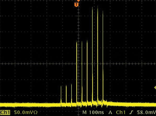
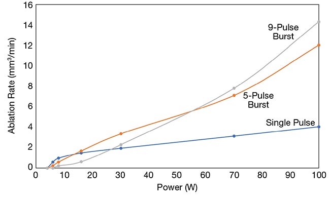
Figure 2. Burst pulses from a high-power IR femtosecond laser with burst envelope tailoring (top). The volumetric ablation rate in stainless steel versus average powers for single-pulse, 5-pulse-burst, and 9-pulse-burst operation (bottom). Courtesy of MKS Instruments.
Optimizing throughput and quality
Micromachining with consistent high quality and minimal heat-affected zones (HAZs) requires laser pulses to be evenly spaced on the workpiece, with an optimized pulse-to-pulse pitch. Additionally, to achieve high throughput, the scanning speeds should be as high as possible throughout a given trajectory. Scanning galvanometer systems are commonly
used and are capable of speeds of tens
of meters per second on relatively long and straight segments. In practice, however, the scanning speed varies widely, depending on the shape of the desired trajectory. Smaller, radiused features
need to be processed at much lower speeds. To maximize throughput with consistent machining quality, an ideal laser source must output pulses (or bursts of pulses) at a controlled frequency that changes in proportion to the variation in trajectory speed, all the while maintaining constant pulse energy and beam parameters.
Systematic control to maintain a constant pulse spacing on the target material while the laser moves at variable speeds is commonly referred to as position-synchronized output (PSO). PSO requires both a motion control system to generate variable frequency electrical trigger pulses and a laser source that is receptive to such pulses. The laser source must also be able to deliver optical pulses with constant energy and beam parameters on demand.
On the motion side, PSO capability is relatively mature for multiaxis linear stage systems and, more recently, has been extended to high-speed galvo
scanner systems. The state of the art for PSO-compatible laser technology, however, has been somewhat less refined, particularly with regard to femtosecond lasers operating at shorter wavelengths,
in which the optical signal typically undergoes a series of transformations in both the temporal and spatial domains.
This situation has begun to change. The development of novel techniques now allows pulse selection, amplification, and harmonic (wavelength) conversion at arbitrary frequencies while maintaining good pulse-to-pulse energy stability and beam quality.
PSO capability can be illustrated with pulsed laser ablation of a target workpiece material. Figure 3 shows microscope images of a polyethylene terephthalate (PET) polymer sample processed with a right-angle corner trajectory at scan speeds of 1, 5, 10 and 15 m/s, without PSO (fixed pulse repetition frequency) and with PSO. In both cases, the laser pulse repetition frequency was specified to maintain a 25-µm pulse spacing on the material at each of the four speeds tested. The results show that without PSO, the spots are more densely spaced at the corners, where the scanner is accelerating and decelerating. Hence, processing without PSO results
in nonuniform spot spacing and depth, high HAZ, and overall poor processing quality — particularly at higher speeds. However, with PSO and the laser adapting the pulse repetition frequency to the variable trigger signal, the spot spacing is maintained at all speeds, resulting in excellent quality and maximum throughput. Note that this level of quality could also be achieved with skywriting processes, but the resulting throughput would be significantly reduced to accommodate the portion of the trajectory where the laser is gated off.
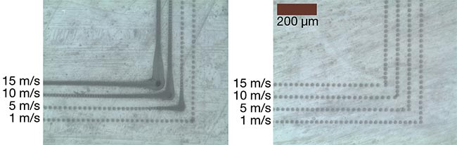
Figure 3. Microscope images of right-angle corners processed in polyethylene terephthalate (PET) using a >50-W femtosecond UV laser without position-synchronized output (PSO) trigger function (left) and with PSO trigger function (right). Courtesy of MKS Instruments.
Advancing key applications
These developments have helped to advance micromachining applications for a range of critical materials. One example is the processing of the polymer films extensively used in consumer electronics, medical devices, and other industrial applications.
Polyimide (PI), for example, is commonly used in microelectronics applications, such as semiconductors, electronic components, displays, image sensors, and lithium-ion batteries. The ability to cut thin PI films with minimum kerf width and low HAZ, and at high speeds, is critical for many of these applications. PET, on the other hand, is a general-use polymer with applications ranging from medical devices to food packaging. As a bulk material, PET is attractive due to its good strength-to-weight ratio and overall break resistance. Similarly, polytetrafluoroethylene (PTFE), commonly known by the trade name Teflon, is another general-use polymer that is resistant to nearly all industrial chemicals and solvents, and that possesses excellent thermal and electrical insulation properties.
Due to their sensitivity to heat, many polymers are difficult to cut and drill at high speeds without the use of high-power UV femtosecond lasers.
Figure 4 shows microscope images of 75-µm-thick PI and PET films and 110-µm-thick PTFE film that were all cut with a >50-W UV femtosecond laser in multipass mode. The laser helped achieve high effective cutting speeds of >300, >500, and ~570 mm/s for the PI, PET, and PTFE films, respectively.
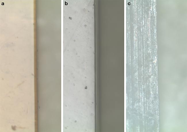
Figure 4. Polyimide (PI) (a) and PET (b) films of 75-µm thickness, and Teflon (c) of 110-µm thickness, all cut with a high-power UV femtosecond laser. Courtesy of MKS Instruments.
Another key market that benefits from advancements in femtosecond lasers is OLED (organic light-emitting diode) displays, which are used for devices ranging from TVs and laptops to smartphones and wearables. OLED technology is also enabling new types of curved, flexible, foldable, and rollable displays that all require new manufacturing processes. Because of the high resolution of OLED screens, for example, the manufacturing process must cut OLED materials with narrow kerf widths and negligible HAZ.
A typical OLED screen comprises a stack of multiple layers, most of which are polymer materials: substrate, anode, conduction, emission, polarizing, cathode, touch sensor, and protective layers. The thickness of each layer ranges from a few to 100 µm, and together they comprise a stack that is typically 300 to 500 µm thick. The layers are bonded together using an optically clear adhesive. Cutting the stack with laser pulses lasting nanoseconds or longer can result in a large HAZ or other quality issues. Moreover, because the properties of the different layers can vary, cutting with IR or green ultrashort-pulse lasers can also be problematic.
Both femtosecond pulse durations and the short wavelength of UV lasers contribute to reduced HAZ, and UV beams also offer tighter focus spot sizes, making narrow cut widths possible.
Figure 5 shows microscope images of a 350-µm-thick OLED film stack cut with
a >50-W UV femtosecond laser in multi-
pass mode, with an effective speed of ~133 mm/s. The clean cuts, with a HAZ of <10 µm, demonstrate that UV femtosecond lasers are well suited for cutting these challenging multilayer film stacks.
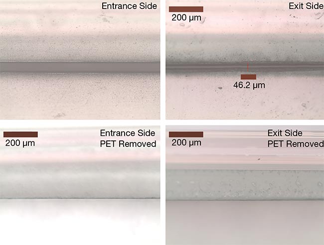
Figure 5. OLED film cut at 133-mm/s effective speed with a UV femtosecond laser at 2-MHz repetition rate. Courtesy of MKS Instruments.
Microelectronics applications
In the semiconductor industry, miniaturization and performance enhancement of electronic products drive the development of new emerging chip fabrication technologies. Thin silicon wafers with thicknesses of 50 to 100 µm enable higher packaging densities and improved heat dissipation. Mechanical saw dicing
causes edge chipping, reduced mechanical stability of the device, and, ultimately, lower throughput and yields. Laser
dicing, which is a contact-free technique, is a compelling solution. However,
the industry demands that the fracture strength of thin silicon wafers be
~1000 MPa. Silicon’s absorption increases linearly toward shorter wavelengths
and nonlinearly toward shorter pulse durations. So, the material favors UV femtosecond lasers for processing thin silicon wafers. Figure 6 shows a microscope image of a thin silicon wafer that was cut with an industrial UV femtosecond laser in multipass mode. A clean cut with a high effective speed of 125 mm/s was demonstrated.
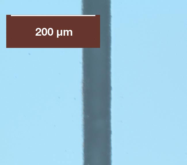
Figure 6. A thin (100-µm) silicon wafer that was cut with a UV femtosecond laser at 125 mm/s. Courtesy of MKS Instruments.
Printed circuit board (PCB) manufacturing has grown in tandem with the market for powerful, rugged, and compact electronic devices. Flexible PCBs are found in large numbers in a wide range
of consumer electronics and are continually being improved through the implementation of new manufacturing arrangements and materials.
Liquid crystal polymer (LCP) is an
increasingly important component of PCBs for high-speed data applications, such as 5G mobile networks. Figure 7 shows microscope images of various
flexible PCB materials cut with an industrial UV femtosecond laser in multipass mode. Bare LCP material of 50-µm
thickness was cut with an effective speed of 500 mm/s. Both a laminate of copper (Cu)-LCP-Cu of 9-50-9-µm thickness and a laminate of Cu-PI-Cu of 12-25-12-µm thickness were cut with an effective
speed of 250 mm/s.
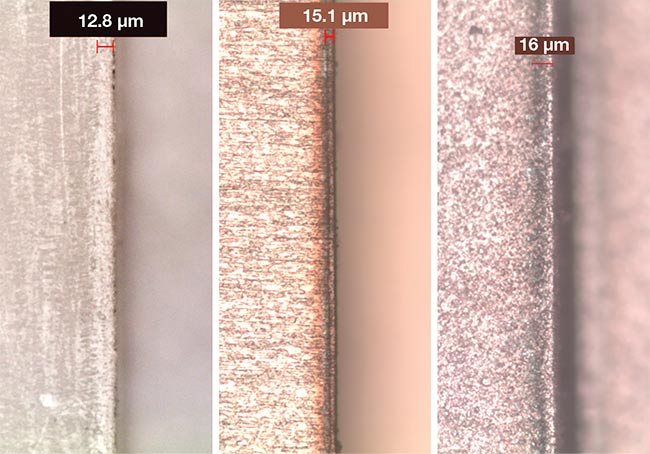
Figure 7. Microscope images of 50-µm-thick bare liquid crystal polymer (LCP) film (left), a copper (Cu)-LCP-Cu stack of 9-50-9-µm thickness (middle), and a Cu-PI-Cu stack of 12-25-12-µm thickness (right) — all cut with a UV femtosecond laser. Courtesy of MKS Instruments.
The recent advancements in femtosecond lasers have delivered benefits encompassing power, pulse repetition frequency, UV wavelengths, burst-mode operation, position-synchronized output capability, reliability, and cost. All of these benefits dovetail with emerging application
demands, such as the need to machine finer features, critical materials, and multilayer film stacks. Together, these converging trends are driving new
opportunities in diverse markets, ranging from semiconductors and PCBs to displays and medical devices. As these trends continue, the future for industrial femtosecond lasers promises exciting possibilities.
Meet the authors
Chandra Nathala is applications engineering manager for Spectra-Physics lasers in Austria; email: [email protected].
Jim Bovatsek is applications engineering manager for Spectra-Physics lasers at MKS Instruments in California; email: [email protected].
Herman Chui is senior director of marketing for the Photonics Solutions Division at MKS Instruments in California; email: [email protected].
Reference
1. B. Neuenschwander et al. (February 2010). Processing of metals and dielectric materials with ps-laser pulses: results, strategies, limitations and needs. Proc SPIE, Vol. 7584, Laser Applications in Microelectronic and Optoelectronic Manufacturing XV, San Francisco, www.doi.org/10.1117/12.846521.